Posts with «digital» label

Various 1 Hz Oscillator Methods

Introduction

During the fun and enjoyment of experimenting with electronics there will come a time when you need a nice 1 Hz oscillator to generate a square-wave signal to drive something in the circuit. On… off… on… off… for all sorts of things. Perhaps a metronome, to drive a TTL clock, blink some LEDs, or for more nefarious purposes. No matter what you need that magic 1 Hz for – there’s a variety of methods to generate it – some more expensive than others – and some more accurate than others.

A few of you may be thinking “pull out the Arduino” and yes, you could knock out a reasonable 1 Hz – however that’s fine for the bench, but wild overkill for embedding a project as a single purpose. So in this article we’ll run through three oscillator methods that can generate a 1 Hz signal (and other frequencies) using methods that vary in cost, accuracy and difficulty – and don’t rely on mains AC. That will be a topic for another day.

Using a 555 timer IC

You can solve this problem quite well for under a dollar with the 555, however the accuracy is going to heavily rely on having the correct values for the passive components. We’ll use the 555 in astable mode, and from a previous article here’s the circuit:

 And with a 5V power supply, here’s the result:

As you can see the cycle time isn’t the best, which can be attributed to the tolerance of the resistors and capacitor C1. A method to increase the accuracy would be to add small trimpots in series with the resistors (and reduce their value accordingly by the trimpot value) – then measure the output with a frequency counter (etc). whilst adjusting the trimpots. If you’re curious about not using C2, the result of doing so introduces some noise on the rising edge, for example:

So if you’ve no other option, or have the right values for the passives – the 555 can do the job. Or get yourself a 555 and experiment with it, there’s lots of fun to be had with it.

Using a GPS receiver module

A variety of GPS modules have a one pulse per second output (PPS) and this includes my well-worn EM406A module (as used in the Arduino tutorials):

With a little work you can turn that PPS output into a usable and incredibly accurate source of 1 Hz. As long as your GPS can receive a signal. In fact, this has been demonstrated in the April 2013 edition of Silicon Chip magazine, in their frequency counter timebase project. But I digress.

If you have an EM406A you most likely have the cable and if not, get one to save your sanity as the connector is quite non-standard. If you’re experimenting a breakout board will also be quite convenient, however you can make your own by just chopping off one end of the cable and soldering the required pins – for example:

You will need access to pins 6, 5, 2 and 1. Looking at the socket on the GPS module, they are numbered 6 to 1 from left to right. Pin 6 is the PPS output, 5 is GND, 2 is for 5V and 1 is GND. Both the GNDs need to be connected together.

Before moving forward you’re probably curious about the pulse, and want to see it. Good idea! However the PPS signal is incredibly quick and has an amplitude of about 2.85 V. If you put a DSO on the PPS and GND output, you can see the pulses as shown below:

 To find the length of the pulse, we had to really zoom in to a 2 uS timebase:

 Wow, that’s small. So a little external circuitry is required to convert that minuscule pulse into something more useful and friendly. We’ll increase the pulse length by using a “pulse stretcher”. To do this we make a monostable timer (“one shot”) with a 555. For around a half-second pulse we’ll use 47k0 for R1 and 10uF for C1. However this triggers on a low signal, so we first pass the PPS signal through a 74HC14 Schmitt inverter – a handy part which turns irregular signals into more sharply defined ones – and also inverts it which can then be used to trigger the monostable. Our circuit:

 and here’s the result – the PPS signal is shown with the matching “stretched” signal on the DSO:

So if you’re a stickley for accuracy, or just want something different for portable or battery-powered applications, using the GPS is a relatively simple solution.

Using a Maxim DS1307/DS3232 real-time clock IC

Those of you with a microcontroller bent may have a Maxim DS1307 or DS3232. Apart from being pretty easy to use as a real-time clock, both of them have a programmable square wave output. Connection via your MCU’s I2C bus is quite easy, for example with the DS1307:

Using a DS3232 is equally as simple. We use a pre-built module with a similar schematic. Once you have either of them connected, the code is quite simple. For the DS1307 (bus address 0x68), write 0x07 then 0x11 to the I2C bus – or for the DS3232 (bus address is also 0x68) write 0x0E then 0x00. Finally, let’s see the 1 Hz on the DSO:

Certainly not the cheapest method, however it gives you an excellent level of accuracy without the GPS.

Conclusion

By no means is this list exhaustive, however hopefully it was interesting and useful. If there’s any other methods you’d like to see demonstrated, leave a comment below and we’ll see what’s possible. And if you made it this far – check out my new book “Arduino Workshop” from No Starch Press.

In the meanwhile have fun and keep checking into tronixstuff.com. Why not follow things on twitterGoogle+, subscribe  for email updates or RSS using the links on the right-hand column? And join our friendly Google Group – dedicated to the projects and related items on this website. Sign up – it’s free, helpful to each other –  and we can all learn something.

The post Various 1 Hz Oscillator Methods appeared first on tronixstuff.

Tronixstuff 31 Jul 14:07
1 hz  555  74hc14  astable  clock  clocks  digital  ds1307  ds3232  em406a  gps  logic  pps  timebase  tronixstuff  ttl  tutorial  

Australian Electronics Nostalgia – Talking Electronics Kits

Introduction

From 1981, Australian electrical engineer Colin Mitchell started publishing his home-grown electronics magazine “Talking Electronics”. His goal was to get people interested and learning about electronics, and more so with a focus on digital electronics. It was (and still is) a lofty goal – in which he succeeded. From a couple of rooms in his home the magazine flourished, and many projects described within were sold as kits. At one stage there were over 150 Talking Electronics kits on the market. You could find the books and kits in retail outlets such as Dick Smith Electronics, and for a short while there was a TE store in Moorabbin (Victoria). Colin and the team’s style of writing was easy to read and very understandable – but don’t take my word for it, you can download the magazines from his website (they’re near the bottom of the left column). Dave Jones recently interviewed Colin, and you can watch those for much more background information.

Over fifteen issues you could learn about blinking LEDs all the way to making your own expandable Z80 board computer, and some of the kits may still be available. Colin also published a series of tutorial books on electronics, and also single-magazine projects. And thus the subjects of our review … we came across the first of these single-issue projects from 1981 – the Mini Frequency Counter (then afterwards we have another kit):

How great is that? The PCB comes with the magazine. This is what set TE apart from the rest, and helped people learn by actually making it easy to build what was described in the magazine instead of just reading about it. For 1981 the PCB was quite good – they were silk-screened which was quite rare at the time:

And if you weren’t quite ready, the magazine also included details of a square-wave oscillator to make and a 52-page short course in digital electronics. However back to the kit…

Assembly

The kit uses common parts and I hoard CMOS ICs so building wasn’t a problem. This (original) version of the kit used LEDs instead of 7-segment displays (which were expensive at the time) so there was plenty of  careful soldering to do:

And after a while the counter started to come together. I used IC sockets just in case:

The rest was straight-forward, and before long 9 V was supplied, and we found success:

To be honest progress floundered for about an hour at this point – the display wouldn’t budge off zero. After checking the multi-vibrator output, calibrating the RC circuits and finally tracing out the circuit with a continuity tester, it turned out one of the links just wasn’t soldered in far enough – and the IC socket for the 4047 was broken So a new link and directly fitting the 4047 fixed it. You live and learn.

Operation

So – we now have a frequency counter that’s good for 100 Hz to the megahertz range, with a minimum of parts. Younger, non-microcontroller people may wonder how that is possible – so here’s the schematic:

The counter works by using a multi-vibrator using a CD4047 to generate a square-wave at 50, 500 and 5 kHz, and the three trimpots are adjusted to calibrate the output. The incoming pulses to measure are fed to the 4026 decade counter/divider ICs. Three of these operate in tandem and each divide the incoming count by ten – and display or reset by the alternating signal from the 4047. However for larger frequencies (above 900 Hz) you need to change the frequency fed to the display circuit in order to display the higher (left-most) digits of the result. A jumper wire is used to select the required level (however if you mounted the kit in a case, a knob or switch could be used).

For example, if you’re measuring 3.456 MHz you start with the jumper on H and the display reads 345 – then you switch to M to read 456 – then you switch to the L jumper and read 560, giving you 3456000 Hz. If desired, you can extend the kit with another PCB to create a 5-digit display. The counter won’t be winning any precision contests – however it has two purposes, which are fulfilled very well. It gives the reader an inexpensive piece of test equipment that works reasonably well, and a fully-documented project so the reader can understand how it works (and more).

And for the curious –  here it is in action:

[Update 20/07/2013] Siren Kit

Found another kit last week, the Talking Electronics “DIY Kit #31 – 9V siren”. It’s an effective and loud siren with true rise and fall, unlike other kits of the era that alternated between two fixed tones. The packaging was quite strong and idea for mail-order at the time:

The label sells the product (and shows the age):

The kit included every part required to work, apart from a PP3 battery, and a single instruction sheet with a good explanation of how the circuit works, and some data about the LM358:

… and as usual the PCB was ahead of its’ time with full silk-screen and solder mask:

Assembly was quite straight-forward. The design is quite compact, so a lot of vertical resistor mounting was necessary due to the lack of space. However it was refreshing to not have any links to fit. After around twenty minutes of relaxed construction, it was ready to test:

It’s a 1/2 watt speaker, however much louder than originally anticipated:

Once again, another complete and well-produced kit.

Conclusion

That was a lot of fun, and I’m off to make the matching square-wave oscillator for the frequency counter. Kudos to Colin for all those years of publication and helping people learn. Lots of companies bang on about offering tutorials and information on the Internet for free, but Colin has been doing it for over ten years. Check out his Talking Electronics website for a huge variety of knowledge, an excellent electronics course you can get on CD – and go easy on him if you have any questions.

Full-sized images available on flickr. This kit was purchased without notifying the supplier.

And if you made it this far – check out my new book “Arduino Workshop” from No Starch Press.

In the meanwhile have fun and keep checking into tronixstuff.com. Why not follow things on twitterGoogle+, subscribe  for email updates or RSS using the links on the right-hand column? And join our friendly Google Group – dedicated to the projects and related items on this website. Sign up – it’s free, helpful to each other –  and we can all learn something.

The post Australian Electronics Nostalgia – Talking Electronics Kits appeared first on tronixstuff.

Tutorial – Arduino and the TI ADS1110 16-bit ADC

Learn how to use the TI ADS1110 16-bit ADC with Arduino in chapter fifty-three of my Arduino Tutorials. The first chapter is here, the complete series is detailed here.

Updated 02/07/2013

Introduction

Moving on from the last chapter where we explained an 8-bit ADC, in this instalment we have the Texas Instruments ADS1110 – an incredibly tiny but useful 16-bit analogue-to-digital converter IC.  It can operate between 2.7 and 5.5 V so it’s also fine for Arduino Due and other lower-voltage development boards. This is a quick guide to get you going with the ADS1110 ready for further applications. Before continuing any further, please download the data sheet (pdf) as it will be useful and referred to during this tutorial. The ADS1110 gives you the option of a more accurate ADC than offered by the Arduino’s 10-bit ADCs – and it’s relatively easy to use. The only block for some is the package type – it’s only available in SOT23-6:

So unless you’re making a customised PCB, some sort of breakout will be required. One useful example is the Schmartboard we reviewed earlier:

The ADS1110 uses the I2C bus for communication, so if this is new to you – please review the I2C tutorials before continuing. And as there’s only six pins you can’t set the bus address – instead, you can select from six variants of the ADS1110 – each with their own address (see page two of the data sheet). As you can see the in the photo above, ours is marked “EDO” which matches to the bus address 1001000 or 0x48h. And with the example circuits we’ve used 10kΩ pull-up resistors on the I2C bus. You can use the ADS1110 as either a single-ended or differential ADC –  But first we need to examine the configuration register which is used to control various attributes, and the data register.

Configuration register

Turn to page eleven of the data sheet. The configuration register is one byte in size, and as the ADS1110 resets on a power-cycle – you need to reset the register if your needs are different to the defaults. The data sheet spells it out quite neatly… bits 0 and 1 determine the gain setting for the PGA (programmable gain amplifier). If you’re just measuring voltages or experimenting, leave these as zero for a gain of 1V/V. Next, the data rate for the ADS1110 is controlled with bits 2 and 3. If you have continuous sampling turned on, this determines the number of samples per second taken by the ADC.

After some experimenting with an Arduino Uno we found the values returned from the ADC were a bit off when using the fastest rate, so leave it as 15 SPS unless required otherwise. Bit 4 sets either continuous sampling (0) or one-off sampling (1). Ignore bits 5 and 6, however they’re always set as 0. Finally bit 7 – if you’re in one-off sampling mode, setting it to 1 requests a sample – and reading it will tell you if the returned data is new (0) or old (1). You can check that the value measured is a new value – if the first bit of the configuration byte that comes after the data is 0, it’s new. If it returns 1 the ADC conversion hasn’t finished.

Data register

As the ADS1110 is a 16-bit ADC, it returns the data over two bytes – and then follows with the value of the configuration register. So if you request three bytes the whole lot comes back. The data is in “two’s complement” form, which is a method of using signed numbers with binary. Converting those two bytes is done by some simple maths. When sampling at 15 SPS, the value returned by the ADS1110 (not the voltage)  falls between -32768 and 32767. The higher byte of the value is multiplied by 256, then added to the lower byte – which is then multiplied by 2.048 and finally divided by 32768. Don’t panic, as we do this in the example sketch below.

Single-ended ADC mode

In this mode you can read a voltage that falls between zero and 2.048 V (which also happens to be the inbuilt reference voltage for the ADS1110). The example circuit is simple (from the data sheet):

Don’t forget the 10kΩ pull-up resistors on the I2C bus. The following sketch uses the ADS1110 in the default mode, and simply returns the voltage measured:

// Example 53.1 - ADS1110 single-sided voltmeter (0~2.048VDC)

#include "Wire.h"
#define ads1110 0x48
float voltage, data;
byte highbyte, lowbyte, configRegister;
void setup()
{
 Serial.begin(9600);
 Wire.begin();
}
void loop()
{
 Wire.requestFrom(ads1110, 3);
 while(Wire.available()) // ensure all the data comes in
 {
 highbyte = Wire.read(); // high byte * B11111111
 lowbyte = Wire.read(); // low byte
 configRegister = Wire.read();
 }

 data = highbyte * 256;
 data = data + lowbyte;
 Serial.print("Data >> ");
 Serial.println(data, DEC);
 Serial.print("Voltage >> ");
 voltage = data * 2.048 ;
 voltage = voltage / 32768.0;
 Serial.print(voltage, DEC);
 Serial.println(" V");
 delay(1000);
}

Once uploaded, connect the signal to measure and open the serial monitor – you’ll be presented with something similar to:

If you need to alter the gain of the internal programmable gain amplifier of the ADC – you’ll need to write a new byte into the configuration register using:

Wire.beginTransmission(ads1110);
Wire.write(configuration byte); 
Wire.endTransmission();

before requesting the ADC data. This would be 0x8D, 0x8E or 0x8F for gain values of 2, 4 and 8 respectively – and use 0x8C to reset the ADS1110 back to default.

Differential ADC mode

In this mode you can read the difference between two voltages that each fall between zero and 5 V. The example circuit is simple (from the data sheet):

We must note here (and in the data sheet) that the ADS1110 can’t accept negative voltages on either of the inputs. You can use the previous sketch for the same results – and the resulting voltage will be the value of Vin- subtracted from Vin+. For example, if you had 2 V on Vin+ and 1 V on Vin- the resulting voltage would be 1 V (with the gain set to 1).

Conclusion

Once again I hope you found this of interest, and possibly useful. And if you enjoy my tutorials, or want to introduce someone else to the interesting world of Arduino – check out my new book “Arduino Workshop” from No Starch Press.

In the meanwhile have fun and keep checking into tronixstuff.com. Why not follow things on twitterGoogle+, subscribe  for email updates or RSS using the links on the right-hand column? And join our friendly Google Group – dedicated to the projects and related items on this website. Sign up – it’s free, helpful to each other –  and we can all learn something.

The post Tutorial – Arduino and the TI ADS1110 16-bit ADC appeared first on tronixstuff.

Tronixstuff 02 Jul 09:06

Tutorial – Arduino and PCF8591 ADC DAC IC

Learn how to use the NXP PCF 8591 8-bit A/D and D/A IC with Arduino in chapter fifty-two of my Arduino Tutorials. The first chapter is here, the complete series is detailed here.

Updated 17/06/2013

Introduction

Have you ever wanted more analogue input pins on your Arduino project, but not wanted to fork out for a Mega? Or would you like to generate analogue signals? Then check out the subject of our tutorial – the NXP PCF8591 IC. It solves both these problems as it has a single DAC (digital to analogue) converter as well as four ADCs (analogue to digital converters) – all accessible via the I2C bus. If the I2C bus is new to you, please familiarise yourself with the readings here before moving forward.

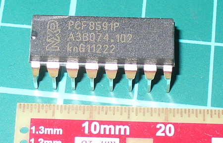
The PCF8591 is available in DIP form, which makes it easy to experiment with:

You can get them from the usual retailers. Before moving on, download the data sheet. The PCF8591 can operate on both 5V and 3.3V so if you’re using an Arduino Due, Raspberry Pi or other 3.3 V development board you’re fine. Now we’ll first explain the DAC, then the ADCs.

Using the DAC (digital-to-analogue converter)

The DAC on the PCF8591 has a resolution of 8-bits – so it can generate a theoretical signal of between zero volts and the reference voltage (Vref) in 255 steps. For demonstration purposes we’ll use a Vref of 5V, and you can use a lower Vref such as 3.3V or whatever you wish the maximum value to be … however it must be less than the supply voltage. Note that when there is a load on the analogue output (a real-world situation), the maximum output voltage will drop – the data sheet (which you downloaded) shows a 10% drop for a 10kΩ load. Now for our demonstration circuit:

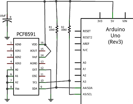
Note the use of 10kΩ pull-up resistors on the I2C bus, and the 10μF capacitor between 5V and GND. The I2C bus address is set by a combination of pins A0~A2, and with them all to GND the address is 0x90. The analogue output can be taken from pin 15 (and there’s a seperate analogue GND on pin 13. Also, connect pin 13 to GND, and circuit GND to Arduino GND.

To control the DAC we need to send two bytes of data. The first is the control byte, which simply activates the DAC and is 1000000 (or 0x40) and the next byte is the value between 0 and 255 (the output level). This is demonstrated in the following sketch:

// Example 52.1 PCF8591 DAC demo
// http://tronixstuff.com/tutorials Chapter 52
// John Boxall June 2013
#include "Wire.h"
#define PCF8591 (0x90 >> 1) // I2C bus address
void setup()
{
 Wire.begin();
}
void loop()
{
 for (int i=0; i<256; i++)
 {
 Wire.beginTransmission(PCF8591); // wake up PCF8591
 Wire.write(0x40); // control byte - turn on DAC (binary 1000000)
 Wire.write(i); // value to send to DAC
 Wire.endTransmission(); // end tranmission
 }

 for (int i=255; i>=0; --i)
 {
 Wire.beginTransmission(PCF8591); // wake up PCF8591
 Wire.write(0x40); // control byte - turn on DAC (binary 1000000)
 Wire.write(i); // value to send to DAC
 Wire.endTransmission(); // end tranmission
 }
}

Did you notice the bit shift of the bus address in the #define statement? Arduino sends 7-bit addresses but the PCF8591 wants an 8-bit, so we shift the byte over by one bit. 

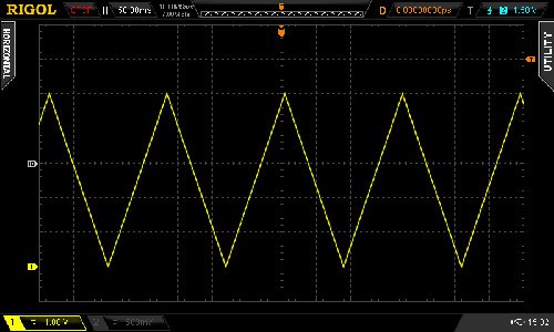
The results of the sketch are shown below, we’ve connected the Vref to 5V and the oscilloscope probe and GND to the analogue output and GND respectively:

If you like curves you can generate sine waves with the sketch below. It uses a lookup table in an array which contains the necessary pre-calculated data points:

// Example 52.2 PCF8591 DAC demo - sine wave
// http://tronixstuff.com/tutorials Chapter 52
// John Boxall June 2013

#include "Wire.h"
#define PCF8591 (0x90 >> 1) // I2C bus address

uint8_t sine_wave[256] = {
 0x80, 0x83, 0x86, 0x89, 0x8C, 0x90, 0x93, 0x96,
 0x99, 0x9C, 0x9F, 0xA2, 0xA5, 0xA8, 0xAB, 0xAE,
 0xB1, 0xB3, 0xB6, 0xB9, 0xBC, 0xBF, 0xC1, 0xC4,
 0xC7, 0xC9, 0xCC, 0xCE, 0xD1, 0xD3, 0xD5, 0xD8,
 0xDA, 0xDC, 0xDE, 0xE0, 0xE2, 0xE4, 0xE6, 0xE8,
 0xEA, 0xEB, 0xED, 0xEF, 0xF0, 0xF1, 0xF3, 0xF4,
 0xF5, 0xF6, 0xF8, 0xF9, 0xFA, 0xFA, 0xFB, 0xFC,
 0xFD, 0xFD, 0xFE, 0xFE, 0xFE, 0xFF, 0xFF, 0xFF,
 0xFF, 0xFF, 0xFF, 0xFF, 0xFE, 0xFE, 0xFE, 0xFD,
 0xFD, 0xFC, 0xFB, 0xFA, 0xFA, 0xF9, 0xF8, 0xF6,
 0xF5, 0xF4, 0xF3, 0xF1, 0xF0, 0xEF, 0xED, 0xEB,
 0xEA, 0xE8, 0xE6, 0xE4, 0xE2, 0xE0, 0xDE, 0xDC,
 0xDA, 0xD8, 0xD5, 0xD3, 0xD1, 0xCE, 0xCC, 0xC9,
 0xC7, 0xC4, 0xC1, 0xBF, 0xBC, 0xB9, 0xB6, 0xB3,
 0xB1, 0xAE, 0xAB, 0xA8, 0xA5, 0xA2, 0x9F, 0x9C,
 0x99, 0x96, 0x93, 0x90, 0x8C, 0x89, 0x86, 0x83,
 0x80, 0x7D, 0x7A, 0x77, 0x74, 0x70, 0x6D, 0x6A,
 0x67, 0x64, 0x61, 0x5E, 0x5B, 0x58, 0x55, 0x52,
 0x4F, 0x4D, 0x4A, 0x47, 0x44, 0x41, 0x3F, 0x3C,
 0x39, 0x37, 0x34, 0x32, 0x2F, 0x2D, 0x2B, 0x28,
 0x26, 0x24, 0x22, 0x20, 0x1E, 0x1C, 0x1A, 0x18,
 0x16, 0x15, 0x13, 0x11, 0x10, 0x0F, 0x0D, 0x0C,
 0x0B, 0x0A, 0x08, 0x07, 0x06, 0x06, 0x05, 0x04,
 0x03, 0x03, 0x02, 0x02, 0x02, 0x01, 0x01, 0x01,
 0x01, 0x01, 0x01, 0x01, 0x02, 0x02, 0x02, 0x03,
 0x03, 0x04, 0x05, 0x06, 0x06, 0x07, 0x08, 0x0A,
 0x0B, 0x0C, 0x0D, 0x0F, 0x10, 0x11, 0x13, 0x15,
 0x16, 0x18, 0x1A, 0x1C, 0x1E, 0x20, 0x22, 0x24,
 0x26, 0x28, 0x2B, 0x2D, 0x2F, 0x32, 0x34, 0x37,
 0x39, 0x3C, 0x3F, 0x41, 0x44, 0x47, 0x4A, 0x4D,
 0x4F, 0x52, 0x55, 0x58, 0x5B, 0x5E, 0x61, 0x64,
 0x67, 0x6A, 0x6D, 0x70, 0x74, 0x77, 0x7A, 0x7D
};
void setup()
{
 Wire.begin();
}
void loop()
{
 for (int i=0; i<256; i++)
 {
 Wire.beginTransmission(PCF8591); // wake up PCF8591
 Wire.write(0x40); // control byte - turn on DAC (binary 1000000)
 Wire.write(sine_wave[i]); // value to send to DAC
 Wire.endTransmission(); // end tranmission
 }
}

And the results:

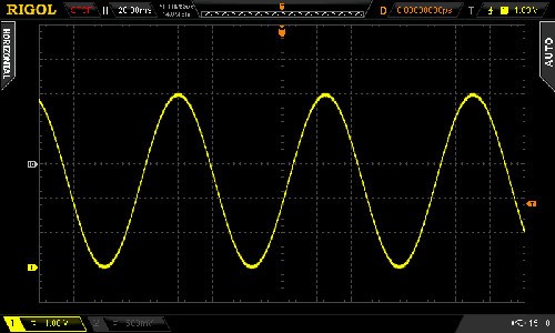
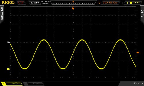
For the following DSO image dump, we changed the Vref to 3.3V – note the change in the maxima on the sine wave:

Now you can experiment with the DAC to make sound effects, signals or control other analogue circuits.

Using the ADCs (analogue-to-digital converters)

If you’ve used the analogRead() function on your Arduino (way back in Chapter One) then you’re already familiar with an ADC. With out PCF8591 we can read a voltage between zero and the Vref and it will return a value of between zero and 255 which is directly proportional to zero and the Vref. For example, measuring 3.3V should return 168. The resolution (8-bit) of the ADC is lower than the onboard Arduino (10-bit) however the PCF8591 can do something the Arduino’s ADC cannot. But we’ll get to that in a moment.

First, to simply read the values of each ADC pin we send a control byte to tell the PCF8591 which ADC we want to read. For ADCs zero to three the control byte is 0x00, 0x01, ox02 and 0x03 respectively. Then we ask for two bytes of data back from the ADC, and store the second byte for use. Why two bytes? The PCF8591 returns the previously measured value first – then the current byte. (See Figure 8 in the data sheet). Finally, if you’re not using all the ADC pins, connect the unused ones to GND.

The following example sketch simply retrieves values from each ADC pin one at a time, then displays them in the serial monitor:

// Example 52.3 PCF8591 ADC demo
// http://tronixstuff.com/tutorials Chapter 52
// John Boxall June 2013
#include "Wire.h"
#define PCF8591 (0x90 >> 1) // I2C bus address
#define ADC0 0x00 // control bytes for reading individual ADCs
#define ADC1 0x01
#define ADC2 0x02
#define ADC3 0x03
byte value0, value1, value2, value3;
void setup()
{
 Wire.begin();
 Serial.begin(9600);
}
void loop()
{
 Wire.beginTransmission(PCF8591); // wake up PCF8591
 Wire.write(ADC0); // control byte - read ADC0
 Wire.endTransmission(); // end tranmission
 Wire.requestFrom(PCF8591, 2);
 value0=Wire.read();
 value0=Wire.read();
 Wire.beginTransmission(PCF8591); // wake up PCF8591
 Wire.write(ADC1); // control byte - read ADC1
 Wire.endTransmission(); // end tranmission
 Wire.requestFrom(PCF8591, 2);
 value1=Wire.read();
 value1=Wire.read();
 Wire.beginTransmission(PCF8591); // wake up PCF8591
 Wire.write(ADC2); // control byte - read ADC2
 Wire.endTransmission(); // end tranmission
 Wire.requestFrom(PCF8591, 2);
 value2=Wire.read();
 value2=Wire.read();
 Wire.beginTransmission(PCF8591); // wake up PCF8591
 Wire.write(ADC3); // control byte - read ADC3
 Wire.endTransmission(); // end tranmission
 Wire.requestFrom(PCF8591, 2);
 value3=Wire.read();
 value3=Wire.read();
 Serial.print(value0); Serial.print(" ");
 Serial.print(value1); Serial.print(" ");
 Serial.print(value2); Serial.print(" ");
 Serial.print(value3); Serial.print(" ");
 Serial.println();
}

Upon running the sketch you’ll be presented with the values of each ADC in the serial monitor. Although it was a simple demonstration to show you how to individually read each ADC, it is a cumbersome method of getting more than one byte at a time from a particular ADC.

To do this, change the control byte to request auto-increment, which is done by setting bit 2 of the control byte to 1. So to start from ADC0 we use a new control byte of binary 00000100 or hexadecimal 0x04. Then request five bytes of data (once again we ignore the first byte) which will cause the PCF8591 to return all values in one chain of bytes. This process is demonstrated in the following sketch:

// Example 52.4 PCF8591 ADC demo
// http://tronixstuff.com/tutorials Chapter 52
// John Boxall June 2013
#include "Wire.h"
#define PCF8591 (0x90 >> 1) // I2C bus address
byte value0, value1, value2, value3;
void setup()
{
 Wire.begin();
 Serial.begin(9600);
}
void loop()
{
 Wire.beginTransmission(PCF8591); // wake up PCF8591
 Wire.write(0x04); // control byte - read ADC0 then auto-increment
 Wire.endTransmission(); // end tranmission
 Wire.requestFrom(PCF8591, 5);
 value0=Wire.read();
 value0=Wire.read();
 value1=Wire.read();
 value2=Wire.read();
 value3=Wire.read();
 Serial.print(value0); Serial.print(" ");
 Serial.print(value1); Serial.print(" ");
 Serial.print(value2); Serial.print(" ");
 Serial.print(value3); Serial.print(" ");
 Serial.println();
}

Previously we mentioned that the PCF8591 can do something that the Arduino’s ADC cannot, and this is offer a differential ADC. As opposed to the Arduino’s single-ended (i.e. it returns the difference between the positive signal voltage and GND, the differential ADC accepts two signals (that don’t necessarily have to be referenced to ground), and returns the difference between the two signals. This can be convenient for measuring small changes in voltages for load cells and so on.

Setting up the PCF8591 for differential ADC is a simple matter of changing the control byte. If you turn to page seven of the data sheet, then consider the different types of analogue input programming. Previously we used mode ’00’ for four inputs, however you can select the others which are clearly illustrated, for example:

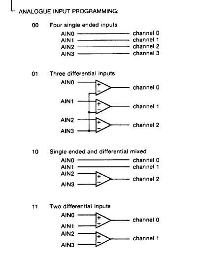
So to set the control byte for two differential inputs, use binary 00110000 or 0x30. Then it’s a simple matter of requesting the bytes of data and working with them. As you can see there’s also combination single/differential and a complex three-differential input. However we’ll leave them for the time being.

Conclusion

Hopefully you found this of interest, whether adding a DAC to your experiments or learning a bit more about ADCs. We’ll have some more analogue to digital articles coming up soon, so stay tuned. And if you enjoy my tutorials, or want to introduce someone else to the interesting world of Arduino – check out my new book “Arduino Workshop” from No Starch Press.

In the meanwhile have fun and keep checking into tronixstuff.com. Why not follow things on twitterGoogle+, subscribe  for email updates or RSS using the links on the right-hand column? And join our friendly Google Group – dedicated to the projects and related items on this website. Sign up – it’s free, helpful to each other –  and we can all learn something.

The post Tutorial – Arduino and PCF8591 ADC DAC IC appeared first on tronixstuff.

Gertboard extender for Raspberry Pi ships to advanced tinkerers

If a seemingly infinitely programmable mini computer like the Raspberry Pi is just too... limiting, we've got good news: the Gertboard extender has started shipping. The $48 companion board reaching customers' doorsteps converts analog to digital and back for Raspberry Pi fans developing home automation, robotics and just about anything else that needs a translation between the computing world and less intelligent objects. The one catch, as you'd sometimes expect from a homebrew project, is the need for some assembly -- you'll have to solder together Gert van Loo's Arduino-controlled invention on your own. We imagine the DIY crowd won't mind, though, as long as they can find the fast-selling Gertboard in the first place.

[Image credit: Stuart Green, Flickr]

Filed under: Misc

Gertboard extender for Raspberry Pi ships to advanced tinkerers originally appeared on Engadget on Wed, 17 Oct 2012 03:58:00 EST. Please see our terms for use of feeds.

Permalink | Email this | Comments