My son wanted to design a circuit to convert microphone inputs to loudness measurements usable by an Arduino (or other ATMega processor). We discussed the idea together, coming up with a few different ideas.
The simplest approach would be to amplify the microphone then do everything digitally on the Arduino. There are several features of this approach:
- The analog circuit is about as simple as we can get: a DC-blocking capacitor and an amplifier. This would only need one op amp, one capacitor, and 2 resistors (plus something to generate a bias voltage—perhaps another op amp, perhaps a low-drop-out regulator).
- Using digital processing, he can do true RMS voltage computation, and whatever low-pass filtering to smooth the result that he wants.
- He can’t sample very fast on the ATMega processor, so high frequencies would not be handled properly. He might be able to sample at 9kHz (about as fast as the ADC operates), but that limits him to 4.5kHz. For his application, that might be good enough, so this doesn’t kill the idea.
- He’d like to have a 60dB dynamic range (say from 50dB to 110dB) or more, but the ADC in the ATMega is only a 10-bit converter, so a 60dB range would require the smallest signal to be ±½LSB, which is at the level of the quantization noise. With careful setting of the gain for the microphone preamp, one might be able to get 55dB dynamic range, but that is pushing it a bit. The resolution would be very good at maximum amplitude, but very poor for quiet inputs.
Although the mostly digital solution has not been completely ruled out, he wanted to know what was possible with analog circuits. We looked at two main choices:
- True-RMS converter chips (intended for multimeters). These do all the analog magic to convert an AC signal to a DC signal with the same RMS voltage. Unfortunately, they are expensive (over $5 in 100s) and need at least a 5v power supply (he is planning to use all 3.3v devices in his design). Also true RMS is a bit of overkill for his design, as log(amplitude) would be good enough.
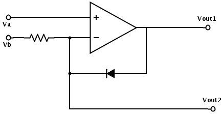
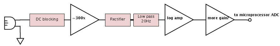
- Using op amps and discrete components to make an amplifier whose output is the logarithm of the amplitude of the input. Together we came up with the following block diagram:

Block diagram of the loudness circuit. (drawn with SchemeIt).
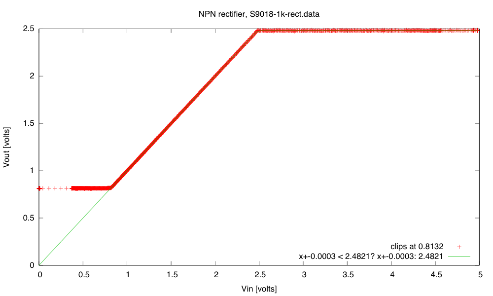
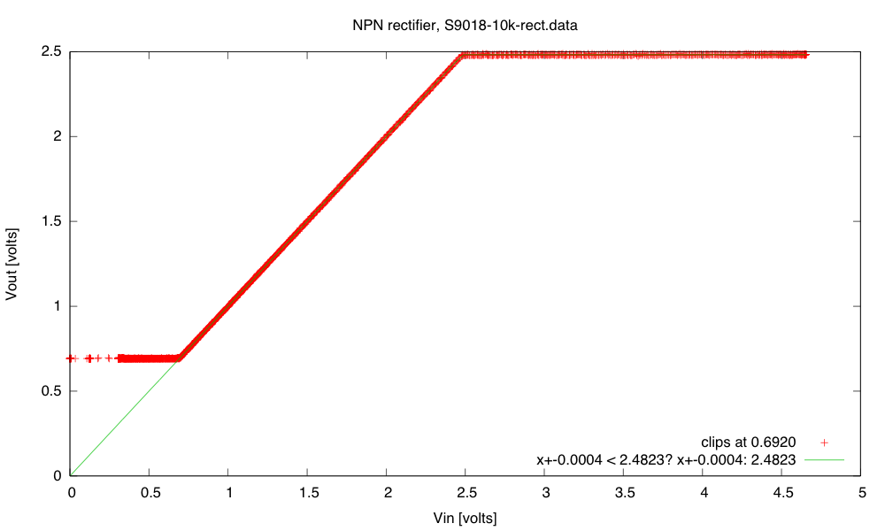
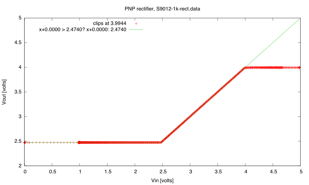
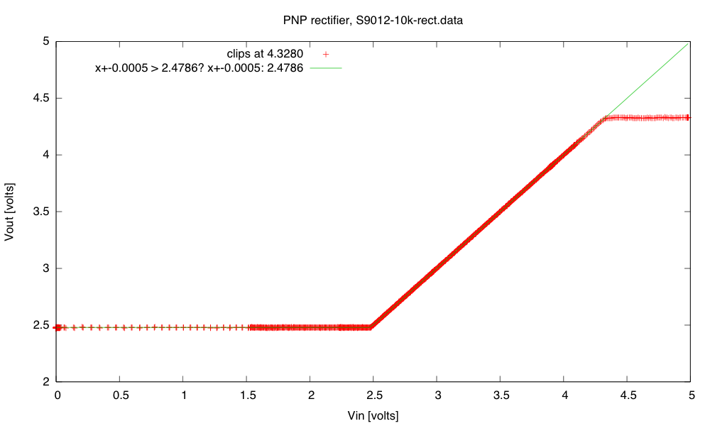
We then spent some time reading on the web how to make good rectifier circuits and logarithmic amplifiers. I’ll do a post later about the rectifier circuits, since there are many variants, but I was most interested in the logarithmic amplifier circuits, which rely on the exponential relationship between current and voltage on a pn junction—often the emitter-base junction of a bipolar transistor.
My son wanted to know what the output range of the log amplifier would be and whether he would need another stage of amplification after the log amplifier. Unfortunately, the theory of the log amplifier uses the Shockley ideal diode equation, which needs the saturation current of the pn junction—not something that is reported for transistors. There is also a “non-ideality” parameter, that can only be set empirically. So we couldn’t compute what the output range would be for a log amplifier.
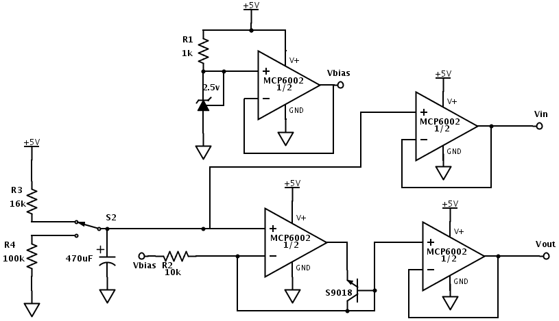
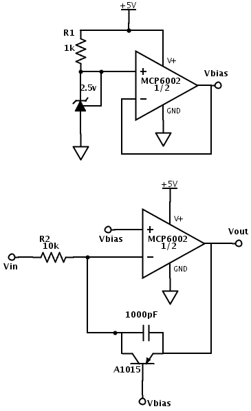
Today I decided to build a log amplifier and see if I could measure the output. I also wanted to figure out what sort of dynamic range he could get from a log amp. Here is the circuit I ended up with, after some tweaking of parameters:

The top circuit is just a bias voltage generator to create a reference voltage from a single supply. I’m working off of 5v USB power, so I set the reference to 2.5v. He might want to use a 1.65v reference, if he is using 3.3v power.
The bottom circuit is the log amplifier itself.
I chose a PNP transistor so that Vout would be more positive as the input current got further from Vbias. I have 6 different PNP transistors from the Iteadstudio assortment of 11 different transistors, and I chose the A1015 rather arbitrarily, because it had the lowest current gain. I should probably try each of the other PNP transistors in this circuit, to see how sensitive the circuit is to the transistor characteristics. I suspect it is very sensitive to them.
The circuit only works if the collector-base junction is reverse-biased (the usual case for bipolar transistors), so that the collector current is determined by the base current. The emitter-base junction may be either forward or reverse biased. Note that if Vin is larger than Vbias, the collector-base junction becomes forward-biased, the negative input of the op amp is slightly above Vbias, and the op amp output hits the bottom rail.
As long as Vin stays below Vbias, the current through R2 should be  , and the output voltage should be
  for some constants A and B that depend on the transistor. Note that changing R2 just changes the offset of the output, not the scaling, so the range of the output is not adjustable without a subsequent amplifier.
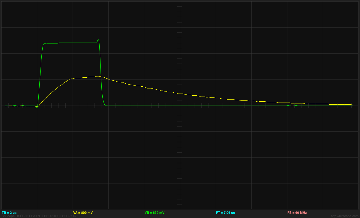
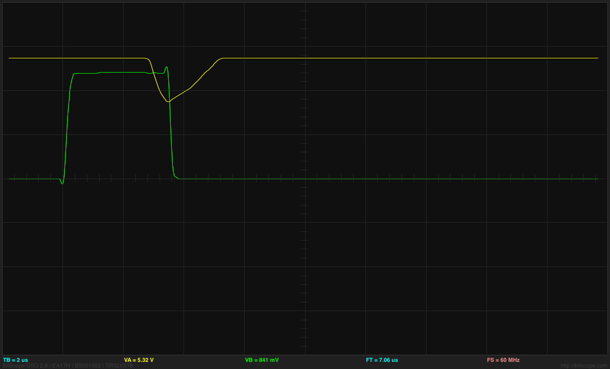
The 1000pF capacitor across the transistor was not part of the designs I saw on the web, but I needed to add it to suppress high-frequency (around 3MHz) oscillations that occurred. The oscillations were strongest when the current through R2 was large, and the log output high. I first tried adding a base-emitter capacitor, which eliminated the oscillations, but I still has some lower-frequency oscillations when the transistor was shutting off (very low currents). Moving the capacitor to be across the whole transistor as shown in the schematic cleaned up both problems.
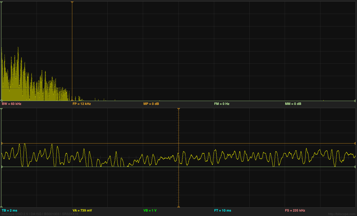
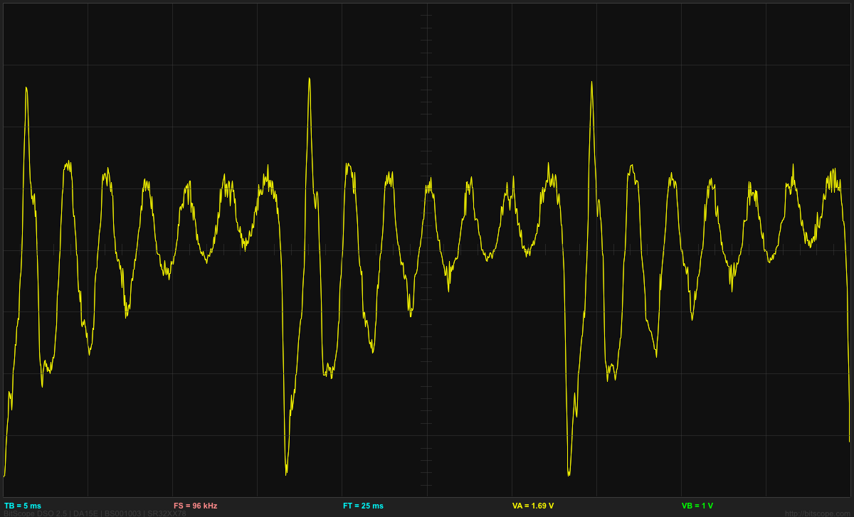
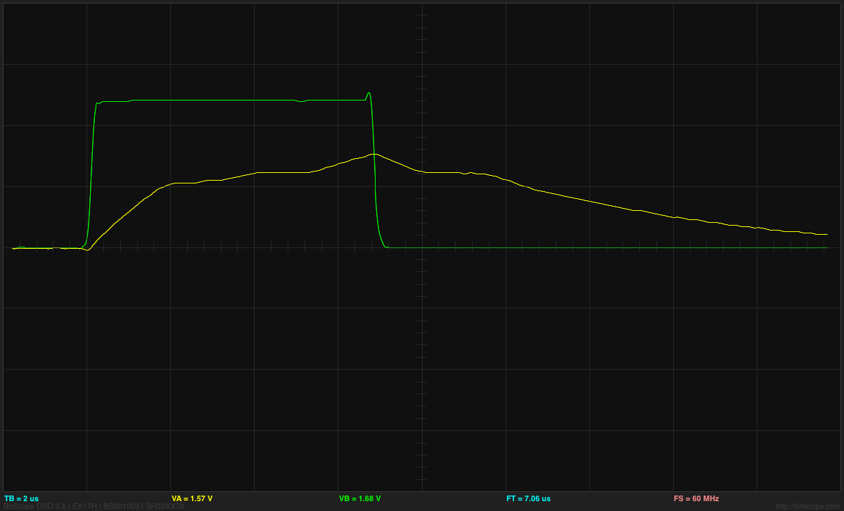
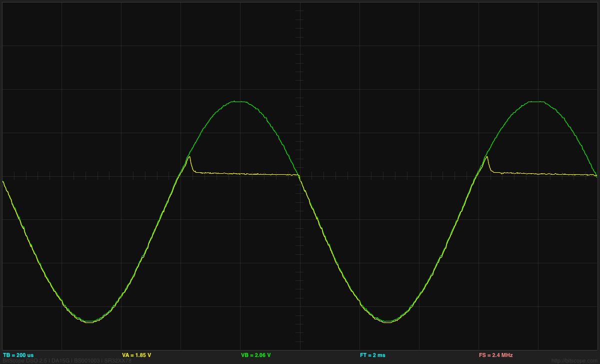
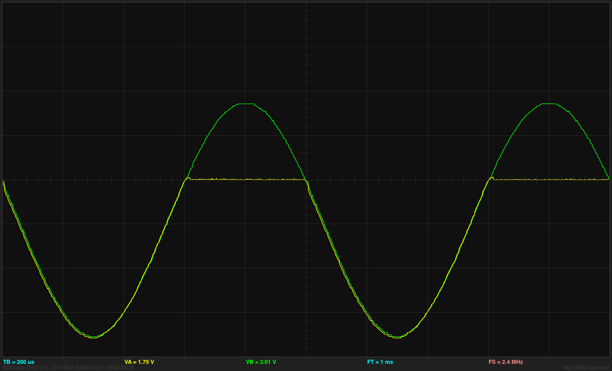
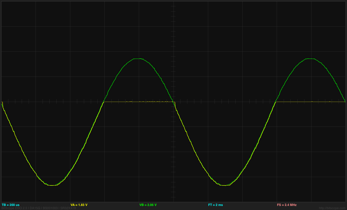
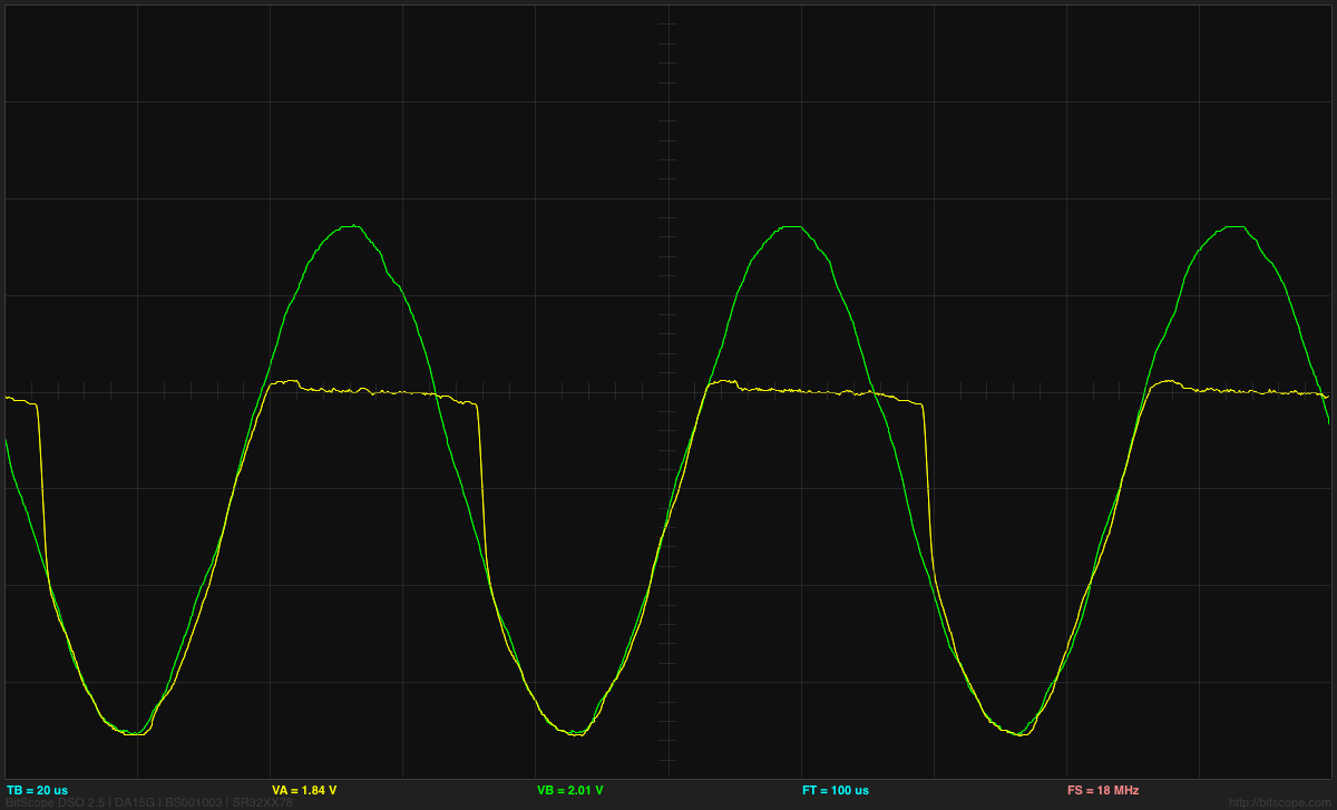
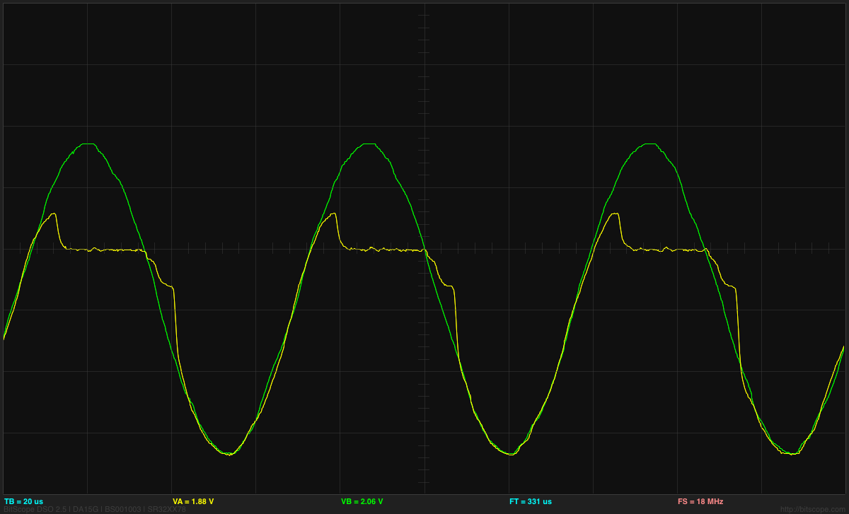
I put ramp and sine wave inputs into the log amplifier. The waveforms were generated with the Bitscope function generator, which does not allow setting the offset very precisely—there is only an 8-bit DAC generating the waveform. Here is a sample waveform:
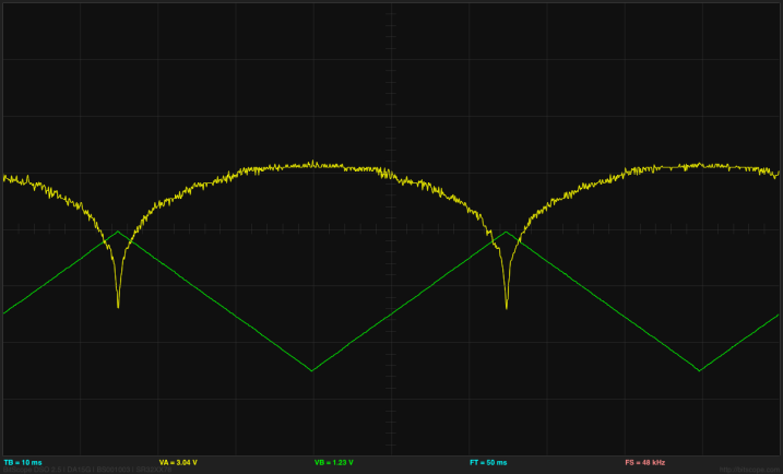
Click picture for larger image. The green trace is the input, the yellow trace is the output. The horizontal axis in the middle is at 2.5V for the input (so the input is always below 2.5V) and at 3V for the output. The scale is 1V/division for the input and 50mV/division for the output. [And all those values should be visible in the saved snapshot, but they aren't.]
The ripple on the output is mainly artifacts of the low-resolution of the BitScope A-to-D converter—smoothing of multiple reads is done, but there is a lot of quantization noise. According to my analog scope there are still some 24MHz noise around, but it seems to be from the Vbias source—adding a 4.7µF capacitor between Vbias and +5V (adjacent pins on the op amp) cleaned things up a lot on the analog scope, without affecting the BitScope traces.
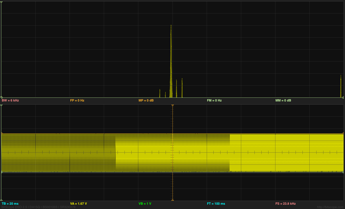
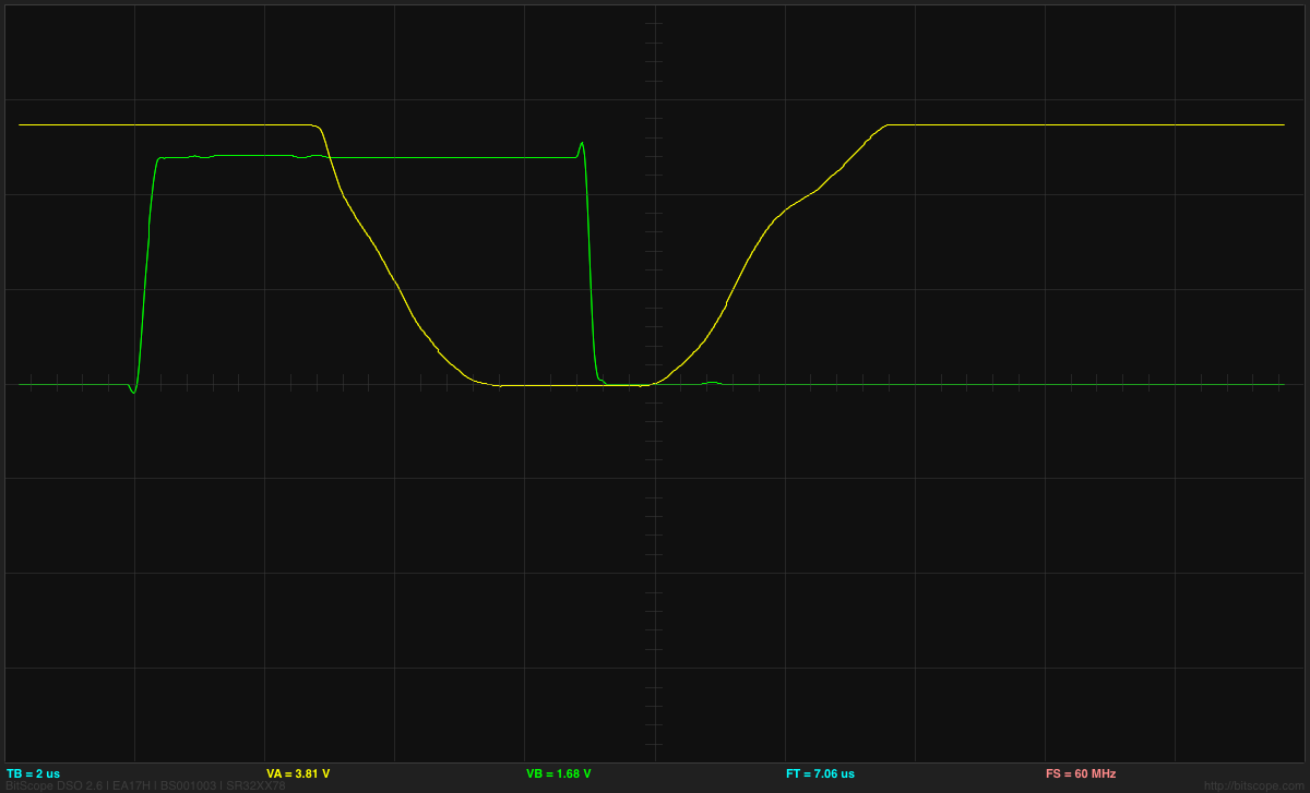
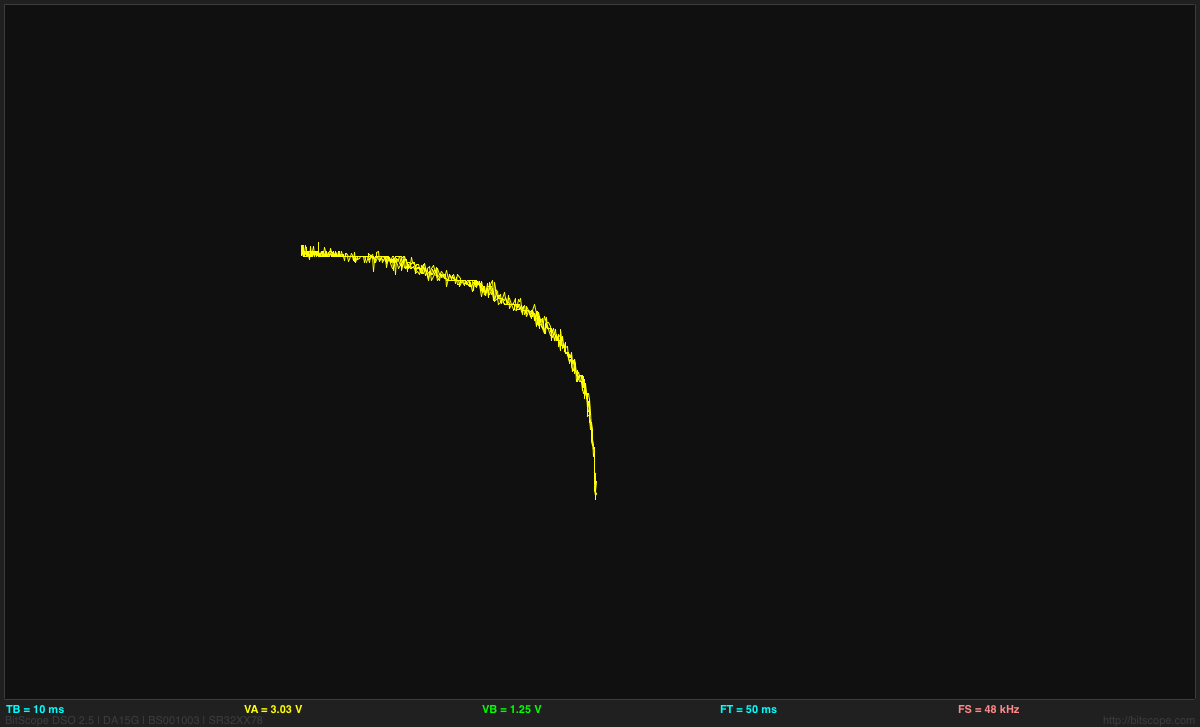
Using the cursors on the BitScope, I was able to measure the output voltages for input voltages of Vbias-0.5V, Vbias-1V, and Vbias-2.5V. From these, I concluded that the scaling factor for the output was about 3.1–3.2 mv/dB. The output was 3±0.07V, so the dynamic range is 140mV/(3.2 mv/dB), or about 44dB. We can see the logarithmic response in an X-Y plot of the output vs the input:

(Click for larger image) Output vs. input of the log amplifier. Note that the output is the log of Vbias-Vin, so the log curve looks backwards here. It’s a shame that BitScope throws away the grid on XY plots, as the axes are still meaningful.
I also tried using an external oscillator, so that I could get better control of the offset voltage, and thus (perhaps) a better view of the dynamic range. I could fairly reliably get an output range of about 200mV, without the hysteresis that occurs when the collector-base junction gets forward biased. That would be over 60dB of dynamic range, which should be fine.
I should be able to adjust the voltage offset of the amplifier by changing R2. Increasing R2 reduces the current, which should lower the voltage. I tried several different values for R2 and measured the maximum output voltage, using the same input throughout:
| 1kΩ |
3.106v |
| 10kΩ |
3.056v |
| 100kΩ |
2.992v |
| 1MΩ |
2.936v |
The 60dB difference in current produces a 170mV difference in output, for 2.83 mV/dB.
Oops, those weren’t quite all the same, as the load from the resistor changes the input. Adding a unity-gain buffer driving the inputs and adjusting the input so that the output of the unity gain buffer has a slight flat spot at 0V gives me a new table:
| 1kΩ |
3.12v |
| 10kΩ |
3.06v |
| 100kΩ |
3.00v |
| 1MΩ |
2.94v |
| 5.6MΩ |
2.90v |
which is consistent with 3mV/dB. I was not able to extend this to lower resistances, as I started seeing limitations on the output current of the op amp. But it is clear that the amplifier can handle a 75dB range of current, with pretty good log response.
An Arduino input is about 5mV/count, so the resolution feeding the output of the log amplifier directly into the Arduino would be about 1.7dB/count. We could use a gain of 4 without saturating an op amp (assuming that we use 2.5V as the center voltage still), for about a 0.4 dB resolution. More reasonably, we could use a gain of 3 to get a resolution of about 0.54dB/count.
I tried that, getting the following table:
| 1kΩ |
4.46v |
| 10kΩ |
4.28v |
| 100kΩ |
4.10v |
| 1MΩ |
3.91v |
| 5.6MΩ |
3.78v |
This table is consistent with 9.1 mv/dB, for a resolution of about 0.54 dB/step on the Arduino.
I tried using the Arduino to collect the same data and fit with gnuplot:

(click plot to see larger version) The gnuplot fit agrees fairly well with the measurements made with the BitScope for 5 resistor values. The resolution of the Arduino DAC limits the ability to measure the dynamic range, and the cloud of points is broad enough to be consistent with slightly different parameter values.
The next thing for me to do on the log amp is probably to try different PNP transistors, to see how that changes the characteristics. My son will probably want to use a surface-mount transistor, so we’ll have to find one that is also available as a through-hole part, so that we can check the log amplifier calibration.
Filed under:
Data acquisition Tagged:
Arduino,
BitScope,
i-vs-v-plot,
log amplifier,
loudness,
op amp 


 , and the output voltage should be
  for some constants A and B that depend on the transistor. Note that changing R2 just changes the offset of the output, not the scaling, so the range of the output is not adjustable without a subsequent amplifier.