

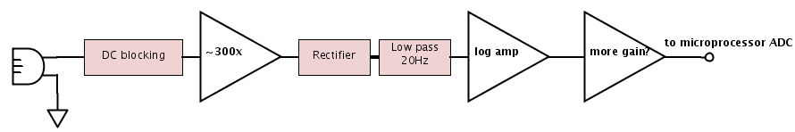
Precision rectifier
The log amplifier that I’ve spent the last several days understanding (posts a, b, c) is not the only non-linear circuit needed for a loudness detector. We also need to convert the audio input signal into a slowly changing amplitude signal that we can take the logarithm of. As I discussed in the first post on log amps, I had rejected true-RMS converter chips as too expensive for the application (though the original application has gone away), and decided to try a rectifier and low-pass filter.
[Incidentally, my son is now looking at a different processor chip, the KL25 from Freescale (an ARM Cortex chip), which has a 16-bit ADC that is much faster than the ATMega’s, so the entire loudness-detector could be done in software, except for a one-op-amp preamplifier. With a 16-bit ADC, we can get almost 90dB of range without needing a log amplifier. We’re planning to order a development board that is compatible with Arduino shields (but has lots more I/O pins available) and that has an accelerometer on the board. Amazingly, the development board is only $13, about half the price of an Arduino.]
A single diode does not work for our rectifier needs in the loudness circuit, because diodes don’t turn on until the voltage across them is at least a “diode drop” (about 0.7v for silicon diodes and 0.45v for Schottky diodes). However, the simple circuit for the log amplifier is also the circuit for a precision rectifier:
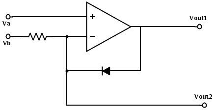
This circuit is both a log amplifier and a precision rectifier. If Vb is set to a constant voltage, then Vout1 varies as log(Vb–Va). Vout2 is max(Va,Vb).
The diode can be connected in the opposite direction, to get Vout2=min(Va,Vb) and Vout1 varying with log(Va–Vb).
The log-amplifier circuit I used in the previous posts had a transistor in place of the diode, so that the crucial voltage that was being exponentiated was referenced to the bias voltage, rather than the input. We also needed a compensation capacitor in parallel with the transistor to prevent oscillation in the negative feedback loop.
For the precision rectifier, we swap the inputs, so that Va is the signal input and Vb is a constant threshold voltage for the rectifier. We do not need (or want) the compensation capacitor, as that would cause the circuit to act as a unity gain amplifier at high frequency, rather than as a rectifier.
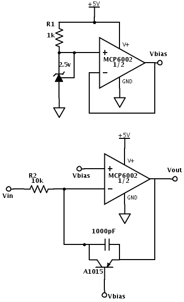
Because I did not happen to have any diodes, but had plenty of transistors, I experimented with the rectifier circuit using diode-connected bipolar transistors (collector and base connected together). Because the output of the rectifier is not directly driven by an op amp, I used unity-gain buffers to isolate the test circuitry (Arduino analog inputs or BitScope oscilloscope) from the amplifier:
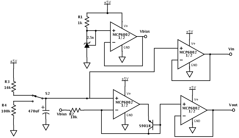
Test circuit for low-speed testing of precision rectifier circuit. Here the NPN transistor is used as a diode, in the opposite direction as in the first schematic, so Vout should be min(Vin, Vbias)
My initial test setup did not have the unity-gain buffer for Vin, but I found that one of my Arduino analog input pins was quite low impedance and was discharging my capacitor. Switching to a different pin helped, but I eventually decided to avoid that kluge and use a unity-gain buffer instead.
I tried several different values for R2. The most predictable effect of changing the value is a change in the range over which the rectifier operates. Clipping occurs because the output of the op amp is limited to be between the rails of the power supply. The feedback transistor is conducting when the rectifier is following the input, so the op amp output has to be substantially lower than Vout. The function implemented is max(Vclip, min(Va,Vbias)). Vclip should go down as R2 is increased (at about 60mV for each factor of 10 in resistance—the same shift as in the log amplifier).
Here are a couple of plots of Vout vs. Vin for the S9018 transistor:
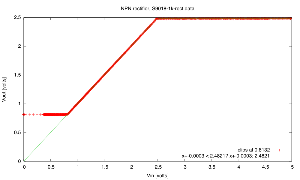
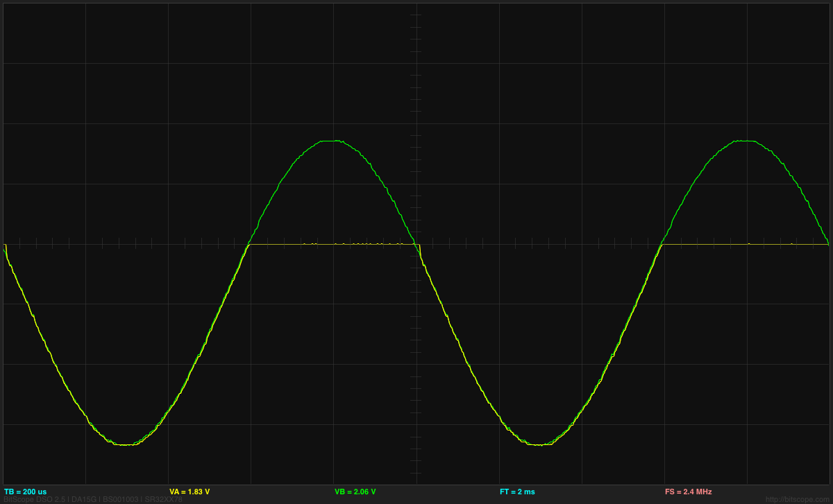
(click to embiggen) With a 1kΩ resistor, the clipping voltage is fairly high, and we have a somewhat limited range for the rectifier. The offset voltage for the rectifier between the output and the input is much less than the resolution of the Arduino ADC (about 5mV).
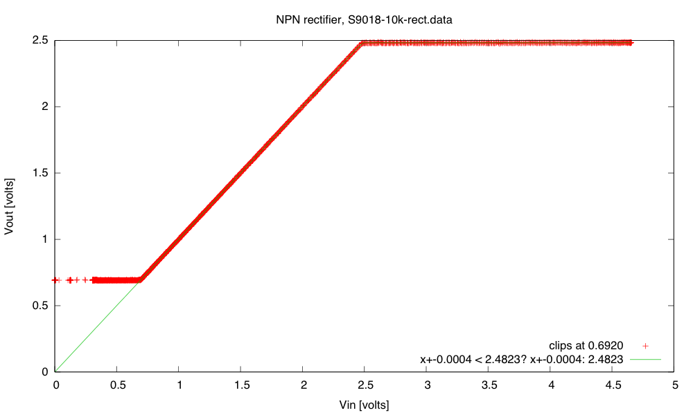
(click to embiggen) With a 10kΩ resistor, the clipping voltage is lower, giving us more range for the rectifier.
Using a PNP transistor instead of an NPN has the effect of reversing the diode and producing Vout=min(Vclip, max(Vin, Vbias)):
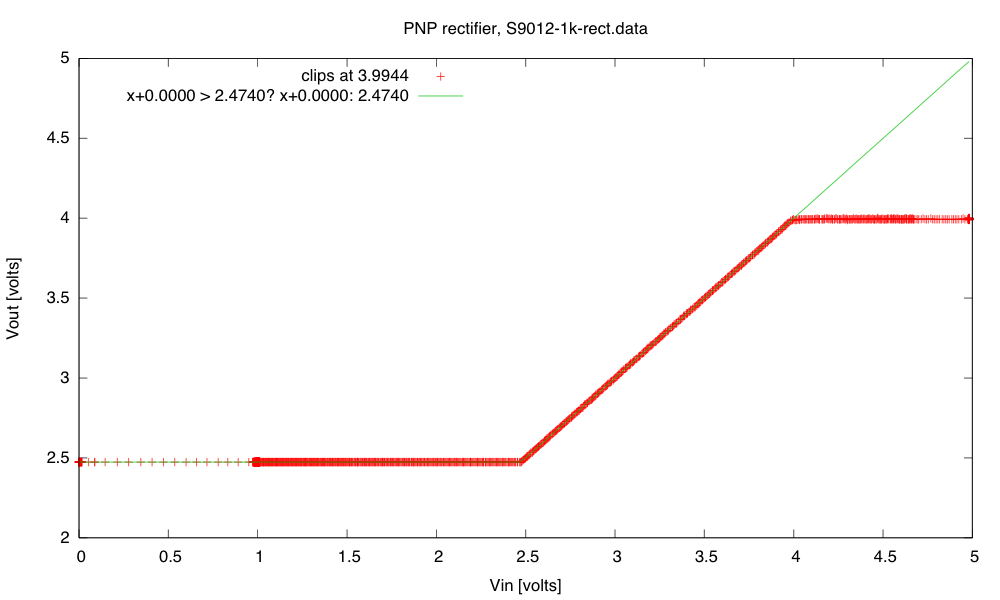
(click to embiggen) With an S9012 PNP transistor and a 1kΩ resistor, we get clipping at the high end.
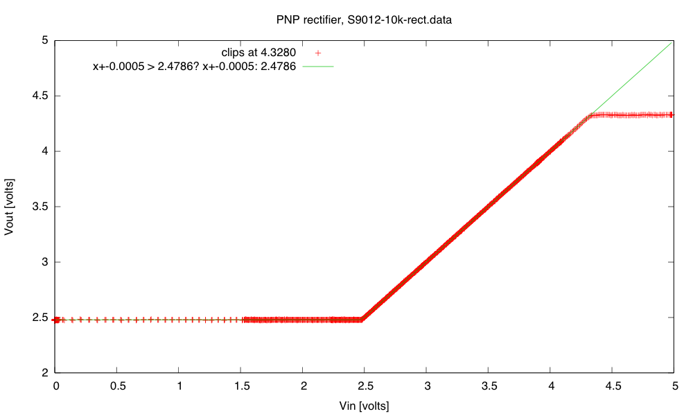
(click to embiggen) With a 10kΩ resistor we get a larger range.
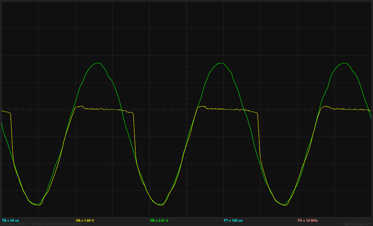
So why not go for a very large resistor and maximize the range? From a DC perspective this looks like a win (though it is hard to see in the limit how Vbias would affect the result if the resistance went to infinity). Of course, the problem is with high-frequency response. Consider the difference between the S9018 NPN transistor with a 1kΩ resistor and a 330kΩ resistor:
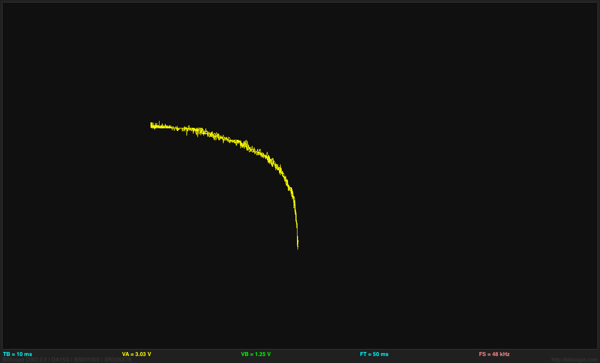
(click to embiggen) With an S9018 NPN transistor and a 330kΩ resistor at 1kHz. Note the overshoot when the rectifier shuts off.
(click to embiggen) Fairly clean signal with a S9018 NPN transistor and a 10kΩ resistor at 1kHz.
(click to embiggen) With a 1kΩ resistor, there is very little overshoot as the rectifier turns off, but we can see a bit of a problem when the rectifier turns back on.
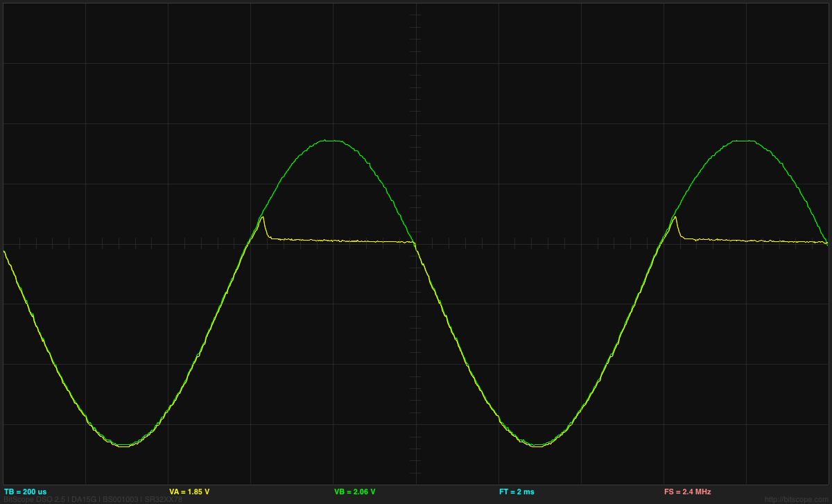
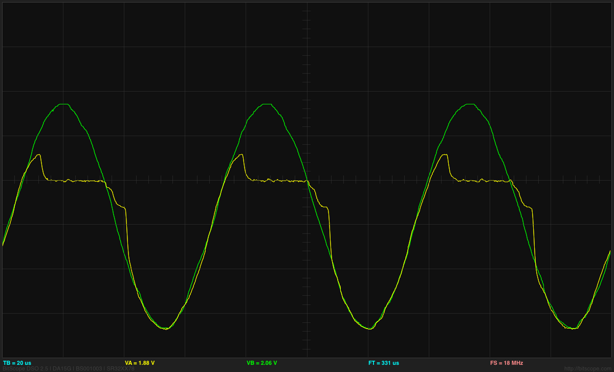
There is a problem with the rectifier turning on slowly, because Vout has to move all the way from the top rail down to the bias voltage, and the op amp has a slew-rate limitation. This phenomenon can be seen more clearly at a higher frequency:
(click to embiggen) The S9018 NPN transistor with a 10kΩ resistor and a 15kHz input signal. The overshoot as the rectifier turns off is about 50mV, and the turn-on delay is about 8µsec. The turn-on delay does not vary much with the input resistance, unlike the turn-off overshoot.
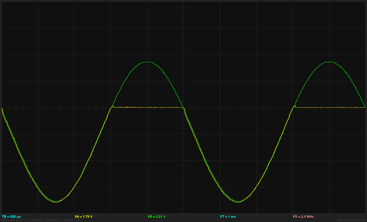
I believe that the overshoot as the rectifier turns off is due to capacitance, as adding a small feedback capacitor in parallel with the diode increases the overshoot substantially:
(click to embiggen) With a 33pF capacitor in parallel with the diode (an S9018 NPN transistor), a 10kΩ resistor, and a 15kHz input, the overshoot goes up to about 290mV from 50mV without the capacitor. The turn-on delay is masked somewhat by the high-frequency feedback.
Note: the S9018 has the best high-frequency response (if you consider 15kHZ high frequency) of any of the transistors I looked, probably because it has the lowest capacitance. For example, with a 10kΩ resistor the S9013 NPN has 120mV of overshoot at 15kHz, instead of only 50mV, and the S9012 PNP has -180mV. With a 1kΩ resistor, I can’t measure the overshoot on any of these three transistors. So the limited range with a 1kΩ resistor is compensated for by the much cleaner turn-off behavior. I should be able to get better range by using a fast-response Schottky diode instead of diode-connected transistor.
Of course, the turn-on behavior is a bigger problem and one that can’t be fixed by playing with the resistor or the diode, because the problem is with the large voltage swing needed from the op amp in order to turn on. There are standard solutions that limit the voltage swing, but I think I’ll leave that for a later blog post.
Filed under: Circuits course, Data acquisition Tagged: Arduino, BitScope, KL25Z, log amplifier, loudness, op amp, rectifier


 , and the output voltage should be
  for some constants A and B that depend on the transistor. Note that changing R2 just changes the offset of the output, not the scaling, so the range of the output is not adjustable without a subsequent amplifier.


 , and the output voltage should be
  for some constants A and B that depend on the transistor. Note that changing R2 just changes the offset of the output, not the scaling, so the range of the output is not adjustable without a subsequent amplifier.

