

Still better I-V plot for Schottky diodes
Last weekend I posted a voltage-versus-current curve for a 1N5817 Schottky diode, to confirm the theoretical formula 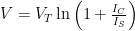

and measuring the results with an Arduino Leonardo. I claimed that the resulting data fits the model well for over six decades (> 120dB):
Fitting over a wide range of currents is more robust than fitting over the narrower range that I can get with just one value for R2.
There is quantization error still on the voltages, but the overlapping current ranges give good data for most of the range. VT is now 26.1mV and IS is 0.91µA.
click to embiggen
I was a little dissatisfied at the low end, because of the low resolution of the Arduino analog-to-digital converter (only 10 bits). This weekend I decided to repeat the measurements, but using a Freedom KL25Z board, which has a 16-bit ADC. Of course, it doesn’t really get 16 bits of accuracy—the data sheet claims that when you use the hardware averaging of 32 samples in 16-bit differential mode (the most accurate) you get at least 12.8 equivalent bits and typically 14.5 equivalent bits. (For single-ended 16-bit, the effective number of bits is only guaranteed to be 12.2, and the typical is 13.9 bits.) They claim a ±6.8LSB total unadjusted error.
My son helped me get the bare metal ARM system set up on my laptop, along with ADC and UART routines, so that I could write my own single-purpose data logger for this problem (he’s working on getting the KL25Z board integrated into the Arduino Data Logger, but it isn’t close to being ready yet). My program used the longest sample times and hardware averaging of 32 samples, to get the most accurate conversions possible from the 16-bit ADC. The first version of the program used differential inputs for the voltage across the diode (E20-E21), but single-ended readings (E21) for the voltage across the resistor. I had to reduce the voltage for the test from 5v to 3.3v, because the KL25Z runs on 3.3v, not 5v. I got some rather weird results:

Two runs of measurement with R2=100Ω. The low-current measurements seem to be all noise.
click to embiggen
I could get decent measurement in the low-current range by using a larger resistor, so the problem was not noise in the measurement fixture or problems reading low differential voltages on the diode, but just with the small single-ended read for the current. It is pretty clear to me that the ADC does not work well when the input voltage results in less than about 50 counts. (Note, that means that at the low end of the voltage range you only have about a 9.4-bit equivalent ADC.)
I modified the circuit to allow differential reading away from 0 for both the voltage across the diode and the voltage across the shunt resistor:

Adding an extra resistor ensured that the lowest voltage did not get too close to ground and I could use differential reads for both voltage (E20-E21) and current (E22-E23)/R2
This gave me a much cleaner reading, with problems only once the differential counts got below about 20:

Differential measurement with R2=100Ω. The low-current measurements have problems when the counts get small, but not nearly as severely as with the single-ended measurements.
click to embiggen
I replaced the 100Ω R2 resistor with a 15.56kΩ resistor (nominally 15kΩ), to extend to lower currents despite the noise in the ADC:

This plot extends the fit down to about 0.1µA, but only by adding an extra term—an offset to the voltage. I thought at first that overshoot to –11mV is an error in the analog-to-digital converter on the KL25Z, as I couldn’t see how my circuit could be back-biasing the diode.
Click to embiggen
I tried using larger resistors, but was unable to get any better data using them—I seem to be limited by the differential voltage measurement of the diode at the low end. I thought I might be able to improve the measurements by adding an instrumentation amp to increase the signal for low voltages. But first I tried just hooking up a voltmeter, with no ADC or instrumentation amp connections. When the voltage across R2 (100kΩ) is 0.31mV, the voltage across the diode plus R2 is only 0.05V, so there is -0.26mV across the diode. The backwards voltage across the diode was not an artifact of the ADC!
I then tried looking at the voltage across the diode with my oscilloscope. There is about 20mV of AC noise, independent of the DC voltage, until the diode has about 50mV across it (with the 15.5kΩ resistor for R2), by which time the noise has dropped to about 10mV (the Bitscope oscilloscope with the differential probe has a noise floor of about 3mV, if the two leads are connected together, so this is not just oscilloscope noise). This noise seems to be white noise, not 60Hz hum pickup, so is probably coming from the diode. This AC noise signal limits how accurately we can measure the DC current, and rectifying the noise could be the source of the mysterious “backwards” bias.
To reduce the noise, I put a 4.7µF ceramic capacitor in parallel with the diode, and redid all the measurements with 100Ω, 15.5kΩ, and 100kΩ resistors for R2.

Modified measurement circuit, adding a bypass capacitor to reduce AC noise on the diode and allow better DC measurement.

Now the signals are very clean down to nanoamp levels. I no longer need to add an offset to the voltage, as it is 0 to within the measurement repeatability. The noise from very small voltage differences for the 100Ω shunt resistor is still a bit of a problem, but that region is well covered by 15.5kΩ data. The curve was fit using just the 15.5kΩ and 100kΩ data, to avoid having to trim out the noise from the 100Ω data.
Click to embiggen
Lessons learned today:
- Higher-resolution ADCs do give smoother curves, with less digitization noise, but they aren’t a panacea for measurement problems. To get most of the resolution, I had to set the ADC to use long sample times and do a lot of averaging. I understand that Freescale Kinetis M series include 24-bit sigma-delta converters for higher precision at much lower speed (24 bits is 7 decimal digits), as well as the high-speed 16-bit successive-approximation converters. Unfortunately, they don’t have a low-cost development board for this series.
- Stay away from the bottom end of the ADC range on the KL25Z. Scale single-ended inputs to have values at least 50, and differential inputs to have values at least 20. There may be similar problems at the top end of the range, but I did not test for them.
I wondered if the problem may be switching from the large value for the voltage across the diode to the small voltage across the shunt resistor that was the problem. I tried putting in a dummy read between the voltage and the current reads, but that didn’t help at all. At first I thought that the low-count readings were good with the large shunt resistors, but this is probably an illusion: errors in the current measurement for small currents aren’t visible on the plot, because the voltage across the diode is not changing, and so large horizontal errors in the plot are not visible there. - Watch out for AC noise when trying to measure DC parameters. If there are semiconductor junctions around, the noise may be rectified to produce an unwanted DC signal.
- The differential ADC settings have a range of ±VDDA, not ±VDDA/2. This means that the least-significant bit step size is twice as big for differential inputs as for single-ended inputs. For some reason the Freescale documentation never bothers to express what the differential range is.
- Serial USB connections are a bit flakey—the Arduino serial monitor missed a byte about every 200–300 lines. I looked for anomalous points on the plot, then commented out the lines that produced them—they were almost all explainable by one character having been missed by the serial monitor; e.g., I commented out “662401069 86 19″ right after “660001069 865 17″, because the last digit of the voltage (the second field) was missing. The fields were a timestamp (in 24MHz ticks), voltage across the diode (in ADC units), and voltage across the shunt resistance (in ADC units). [Actually, this was not a new lesson for me—I've had to do the same on almost all files collected from the Arduino serial monitor. My son's data logger code is better at not losing data, but it is still worthwhile to check for anomalies.]
- The 3.3v supply from the Freedom board is much cleaner than the 5v USB supply that I get from the Arduino (unless I use an external power supply with the Arduino), but I can only take about 10mA from the 3.3v supply before it begins to droop. If I want more than that, I’d better provide my own power supply (or at least my own LDO regulator from the USB 5v supply).
Filed under: Circuits course, Data acquisition Tagged: Arduino, i-vs-v-plot, KL25Z, Schottky diode


 , where IS is the saturation current of the diode, using the following setup


 for some constant x. Note that if we leave the –1 in, then we’ll have a small DC offset to iC.
 is temperature-dependent, since
  , which is about 26mV at 300˚K. The scale factor can be multiplied by ln(10) to get 60mV/decade or 3mv/dB.
 will be poor. If I make R2 small, the current may exceed what the transistor is designed for and there may be saturation effects.

 .
. , and we could make arbitrary tradeoffs between v2 and RC.


