Yesterday, I spent the day testing different transistors in the log amplifier, to see whether it made much difference which transistor I used. I wanted to test all 11 transistors in the iteadstudio assortment, the 5 PNP transistors and the 6 NPN transistors, to see if it made much difference and whether one of the transistors would give me a larger mV/dB scaling than the others.
Here is the test circuit I made (essentially the same as for the tests in Logarithmic amplifier again):

(click image to embiggen) The same circuit can be used for either NPN or PNP transistors. The only difference is whether the 470µF capacitor starts at 0v (for PNP) or 5v (for NPN) before decaying to Vbias through the 16kΩ resistor R5. For many of the tests the voltage-to-current resistor R2 was 1kΩ rather than 10kΩ.
The op amp at the top is a unity-gain buffer to provide a steady Vbias source that capable of providing some current (unlike the TL431ILP voltage reference shown here as an adjustable Zener diode). The nominal 2.5V reference was closer to 2.48V, which is within the ±2% spec for the part.
The unity-gain buffer on the left is to make the load on the RC circuit as high impedance as possible, so as not to disrupt the RC charging or discharging. The input current of the MCP6002 is typically ±1pA, which is far smaller than other sources of error (such as the parallel resistance of the capacitor itself). The parallel resistance of the capacitor makes the destination voltage of the RC circuit slightly lower than Vbias, which means that we will not get all the way to Vbias when testing PNP transistors, but will overshoot slightly when testing NPN transistors. (We should be able to reverse that by putting the capacitor between +5V and the switch, rather than ground and the switch.)
The right-hand op amp is just a non-inverting amplifier with 3× gain, to get better precision on measuring the output voltage with the Arduino ADC. I made some measurements with Vout but most with the 3Vout signal. The scaling factor was 3.0 much more accurately than the repeatability of my fits to the data, so the gain in precision was not accompanied by a loss of accuracy. Ideally, I’d like to be able to use more than a 3× gain in the final stage, to get better precision, but I’m limited by the offset voltage of the log amplifier, which is determined by the transistor and by the voltage-to-current converter R2.
The middle op amp is the log amplifier itself, which relies on the exponential relationship of the emitter current to the voltage across the base-emitter junction. More precisely, we can use the Ebers-Moll model of a bipolar transistor to get

The collector is held at Vbias by the feedback loop of the op amp, so VBC is zero, simplifying the equation to

Assuming that βR and IS are constant, and that VBE is very large compared to VT (about 23 times bigger in my measurements), we have the desired exponential relationship:  for some constant x. Note that if we leave the –1 in, then we’ll have a small DC offset to iC.
(I believe that all this analysis is correct for NPN transistors, where VBE is positive, but that some signs may need to be negated for PNP transistors.)
The log-amplifier output  is temperature-dependent, since
  , which is about 26mV at 300˚K. The scale factor can be multiplied by ln(10) to get 60mV/decade or 3mv/dB.
Note that this scaling is not affected by the current gain β of the transistor—that only affects the offset of the output voltage. This analysis agrees with the statement in Wikipedia, “At room temperature, an increase in VBE by approximately 60 mV increases the emitter current by a factor of 10.” There is probably an even bigger temperature dependence for the offset of the output than for the scaling, because of changes in βR and IS, but that is not included in the Ebers-Moll model.
The theoretical result indicates that I should get about 3mV/dB for any transistor, but that the offset voltage will vary depending on the characteristics of the transistor. I might also run into effects not included in the Ebers-Moll model, especially at very large or very small collector currents.
Adjusting R2 to change the current can move the output offset around. If I make R2 large and the current small, then VBE will be small, and the approximation  will be poor. If I make R2 small, the current may exceed what the transistor is designed for and there may be saturation effects.
Looking at typical collector currents on the I-vs-V plots for the transistors, I’m seeing values like 8–20mA at the high end, so with a 2.5V drop across R2, I want R2 to be at least 300Ω. Initially, I picked 1kΩ, as providing a large current at 2.5V, hoping that this would give a large dynamic range. Here are a couple of good examples of measurements using the 3× output and R2=1kΩ.

(click image to embiggen) Typical 3× Vout vs Vin curve for a PNP transistor, here the A1015, using R2=1kΩ. This uses Arduino-measured Vin, Vout, and Vbias, so is limited to about 2 decades (40dB).

(click image to embiggen) Typical 3× Vout vs. Vin curve for an NPN transistor, using R2=1kΩ. Again we’re limited by the Arduino ADC to about 40dB of dynamic range.
The exponential decay of the capacitor to about Vbias allows us to extend the range of the fit well past the resolution of the ADC to measure Vin or Vbias. Combining the formulas for the log amplifier and the RC discharge gives us the general formula
 .
.
Fitting the constants for this turns out to be difficult, because v3 is close to zero. If it were exactly zero, the formula would be  , and we could make arbitrary tradeoffs between v2 and RC.
We can get a nice plot of Vout vs. time as the capacitor decays toward Vbias, particularly for the NPN transistor S9013:

(click picture to embiggen) The S9013 log amplifier shows what looks like a good fit over about 80dB, when using R2=1kΩ, and good linearity for about 65dB. The upward tail shows where the collector-base junction begins to be forward biased, and the current is no longer controlled by the base-emitter voltage.
Note that this curve shows that the problems we had with direct measurement of RC discharge curves in the physics lab was due to limitations of the Arduino ADC, not to the underlying RC circuit. The tails of the discharge continue to follow the exponential well beyond the resolution of the 10-bit ADC in the Arduino.
Of course, I picked out the S9013 plot to show, because it was the nicest one. Some of the others were weird. For example, consider the 2N5551:
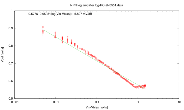
(click image to embiggen) Not that the 2N5551 Vout vs Vin curve is not a simple logarithm—there is some sort of saturation happening for large input voltages, so the straight-line fit is awful.
The same 2N5551 transistor with R2 at 10kΩ behaves much better:

(click image to embiggen) With a 10kΩ resistor, the currents through the 2N5551 transistor are smaller, and no clipping occurs.
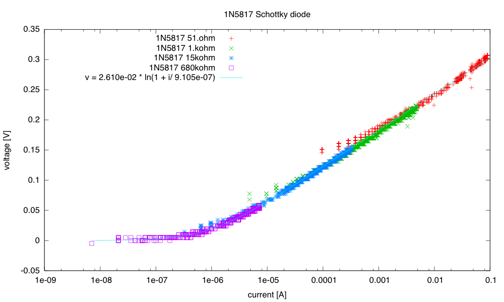
Even weirder was the behavior of the S9018 NPN transistor (the only transistor in the set not matched by a corresponding PNP transistor):

(click image to embiggen) With R2=1kΩ, the S9018 transistor shows a flat spot in the response for 277mV < Vin-Vbias < 330mV (that is, 277uA < IC < 330uA) . I have no idea what causes this flat spot.
I’m still mystified by the flat spot in the S9018 response—anyone have any ideas??
By changing R2 to 10kΩ, we can push the flat spot to 10× higher voltage, just outside the input range that the log amplifier uses:

(click image to embiggen) With R2=10kΩ, the response of the amplifier with a S9018 transistor is nicely logarithmic.
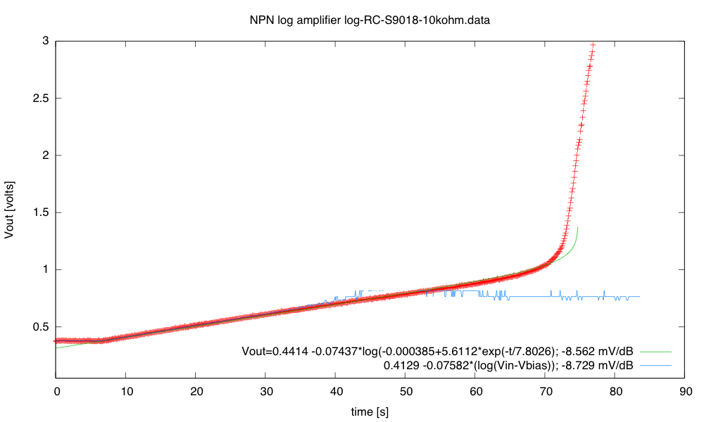
The time response to the RC discharge also looks good:

(click to embiggen) With R2=10kΩ, we get a good fit for about 76dB on the S9018 transistor. The larger resistor gives a somewhat softer turn on for the transistor if we go past Vbias.
All of my transistors gave mV/dB scaling that was about the same (just under 9 mV/dB after the 3× gain, so just under 3mV/dB for the unamplified output), as is predicted by the Ebers-Moll model. I got better dynamic ranges for the NPN transistors than for the PNP transistors, but this may have been due to artifacts of the test setup. In any case, it looks like 60–70dB ranges are fairly easily achieved.
[UPDATE 2013 July 15: I know I said I was done with the log amplifiers, but I had to do just one more test. In addition to the 16kΩ resistor to Vbias, I added a 5.7MΩ resistor to +5V, giving me a slightly higher target voltage so that I had some overshoot when testing PNP transistors. With this setup I could test the S9012 PNP transistor for 82dB with R2=1kΩ, and 63dB with R2=10kΩ. So the better dynamic range of the NPN was just an artifact of my test setup, as I thought.]
If one were to try to make a measuring instrument with a log amplifier, there would have to be some temperature compensation as the log-amplifier offset and scaling are both temperature sensitive. Having a temperature-independent voltage source for calibration would be a good idea.
I think I’m about burned out on log amplifiers now. Perhaps later his week I’ll try doing some precision rectifier circuits.
Filed under:
Circuits course,
Data acquisition Tagged:
Arduino,
bipolar transistors,
i-vs-v-plot,
log amplifier,
op amp 


 , where IS is the saturation current of the diode:


 for some constant x. Note that if we leave the –1 in, then we’ll have a small DC offset to iC.
 is temperature-dependent, since
  , which is about 26mV at 300˚K. The scale factor can be multiplied by ln(10) to get 60mV/decade or 3mv/dB.
 will be poor. If I make R2 small, the current may exceed what the transistor is designed for and there may be saturation effects.

 .
. , and we could make arbitrary tradeoffs between v2 and RC.


