Posts with «fpga» label

Arduino Does SDI Video with FPGA Help

If you are running video around your home theater, you probably use HDMI. If you are running it in a professional studio, however, you are probably using SDI, Serial Digital Interface. [Chris Brown] looks at SDI and shows a cheap SDI signal generator for an Arduino.

On the face of it, SDI isn’t that hard. In fact, [Chris] calls it “dead simple.” The problem is the bit rate which can be as high as 1.485 Gbps for the HD-SDI standard. Even for a super fast processor, this is a bit much, so [Chris] turned to the Arduino MKR Vidor 4000. Why? Because it has an FPGA onboard. Alas, the FPGA can’t do more than about 200 MHz, but that’s fast enough to drive an external Semtech GS296t2 serializer which is made to drive SDI signals.

The resulting project contains the Arduino, the serializer, a custom PCB, and both FPGA and microcontroller code. While the total cost of the project was a little under $200, that’s still better than the $350 to $2000 for a commercial SDI signal generator.

If you want to play along, the files are out on GitHub. We used the Vidor back in 2018 when it first came out. If you need a quick start on FPGAs, there’s always our boot camp.

17 Fun Projects for New Boards from Raspberry Pi, Arduino, Micro:Bit, and More

When a new board drops, makers around the planet immediately start hacking new projects with it. Here are 17 fun projects to try on fresh hardware.

The post 17 Fun Projects for New Boards from Raspberry Pi, Arduino, Micro:Bit, and More appeared first on Make: DIY Projects and Ideas for Makers.

Arduino and FPGA Done Differently

FPGA guru [Max Maxfield] recently took a look at the XLR8 (pronounced accelerate) board from a company called Alorium. On the surface, it looks like another Arduino UNO clone. But instead of a CPU, it contains an Intel MAX10 FPGA that runs a softcore

AVR processor. Of course, that’s only part of the story. If the board was just a mock Arduino using an FPGA, that’s not very interesting for practical purposes. However, by incorporating accelerator blocks or XBs, you can add FPGA modules to the soft CPU. [Max] shows an example that you can see in the video below where an FPGA block controls servos more easily than a standard Arduino. There’s also a version that looks like an Arduino Nano, but can clock much faster as well as use the XBs.

In addition to prebuilt XBs, there is a workflow to build your own if you are familiar with working with FPGAs. The products aren’t exactly new, but we enjoyed [Max’s] take on the product. We also appreciated the simple code examples showing exactly how you would convert a program to use the accelerated functions.

The idea isn’t new or original, of course. You might argue that Arduino’s official FPGA support should have worked like this. The comments on the post also talk about several similar boards from earlier that never gained much traction, including ZPUino.

We talked about the nano-like board a few years ago. We’ve seen projects with the ZPUino before, too.

Hack a Day 21 Mar 15:01

Make Room For A New Arduino Competitor – With Native Brainf*ck!

With so many smaller and more capable microcontroller boards on the market it’s now fairly safe to say that the classic Arduino footprint and form factor is rather outdated. That’s not to say that there’s no fight left in the old contender though, and to prove it here’s a new platform in the familiar style set by the venerable Atmel-based board. [Eduardo Corpeño]’s Brainfuino is an Arduino competitor that runs everyone’s favourite esoteric programming language, Brainf*ck. (Keeping it SFW, folks.)

And in case you mistake it for a Brainf*ck emulator on a PCB then stand ready to be corrected, for this board runs the language natively in a Brainf*ck softcore on a Lattice MachXO2 FPGA. This is the real deal, on which only a true genius or masochist would dare to code.

The board itself is very neatly executed with a graphical style that presents more than a nod to the original Arduino. On this board is the FPGA, 256 kB ROM and 138 kB RAM, an STM32 to provide a USB serial port and an analogue input, and a level shifter to provide Arduino-style 5 V logic on the pins. We can see it’ll provide hours of fun to anyone interested in learning Brainf*ck, but besides that it has potential as an Arduino-shaped FPGA board. We like the joke, we like the graphical and engineering design, but underneath that lies quite the technical achievement.

Brainf*ck has made it to Hackaday before, not least in this jaw-dropping relay computer.

Hack a Day 12 Jan 09:00
arduino  brainfuck  fpga  

Upgrading a MIDI Controller with an FPGA

While the “M” in MIDI stands for “musical”, it’s possible to use this standard for other things as well. [s-ol] has been working on a VJ setup (mixing video instead of music) using various potentiometer-based hardware and MIDI to interface everything together. After becoming frustrated with drift in the potentiometers, he set out to outfit the entire rig with custom-built encoders.

[s-ol] designed the rotary-encoder based boards around an FPGA. It monitors the encoder for changes, controls eight RGB LEDs per knob, and even does capacitive touch sensing on the aluminum knob itself. The FPGA communicates via SPI with an Arduino master controller which communicates to a PC using a serial interface. This is [s-ol]’s first time diving into an FPGA project and it looks like he hit it out of the park!.

Even if you’re not mixing video or music, these encoders might be useful to any project where a standard analog potentiometer isn’t accurate or precise enough, or if you just need something that can dial into a specific value quickly. Potentiometers fall short in many different ways, but if you don’t want to replace them you might modify potentiometers to suit your purposes.

Hands on with the Arduino FPGA

All of the tools you need to work with the FPGA Arduino — the Vidor — are now in the wild!

We reported earlier that a series of French blog posts finally showed how all the pieces fit together to program the FPGA on the Arduino MKR4000 Vidor board. Of course, I wasn’t content to just read the Google translation, I had to break out the board and try myself.

I created a very simple starter template, a tool in C to do the bitstream conversion, required, and bundled it all together in one place. Here’s how you can use my starter kit to do your own FPGA designs using the Vidor. I’m going to assume you know about FPGA basics and Verilog. If you don’t, why not check out the FPGA boot camps first?

The first thing you’ll want to do is grab my GitHub repo. You’ll also need the Arduino IDE (a recent copy) and Intel’s Quartus software. Inside, you’ll find three directories, two of which contain slightly modified copies of original Arduino files. But before you start digging in, let’s get the high-level overview of the process.

Basic Concepts

The FPGA onboard the Vidor is an Intel/Altera device so to configure it, we’ll use Quartus. Usually, Quartus handles everything including programming the device, but we can’t use it for that with the Vidor. Instead, we will have to tell the CPU how we want the FPGA configured and it will do it for us as part of our Arduino program (I really hate saying sketch).

Quartus (see below) will take our Verilog files and create a ttf file that represents the configuration bitstream. This is just an ASCII text file full of decimal numbers. Unfortunately, the way the Vidor is set up, it needs the numbers bit reversed at the byte level. That is, 01 in the ttf file needs to be 80 hex sent to the FPGA.

Arduino supplies a Java class file to do the task, but I got frustrated because the class file needed Java 11 and I didn’t want to put it on every machine I use, so I just rewrote it in C. It is easy enough to port the algorithm, though. In the shell subdirectory, I have another example implementation using awk.

Once you have this stream of numbers, you can include it in an Arduino sketch with some boilerplate to enable the FPGA and load it. The standard program includes the file app.h which is just the output of the conversion program. There’s no C code in it, just comma-separated numbers that the main code will stick in an array at compile-time. Beyond that, it is a normal Arduino program and you can do what you like. Upload it and you’ll get the CPU and FPGA programmed all in one go.

There is one caveat. The FPGA code has a top-level block with lots of I/O pins defined and the corresponding constraints. You should be very careful not to change these or alter the pin constraints. If you drive a pin that’s already an output, for example, you could do real harm to the board. Because all the pins are shared, you have the same problem with the Arduino pins, too. If you are driving an output pin with the FPGA, you shouldn’t try to drive it with the CPU also. However, as you will see, it is perfectly fine to have the FPGA reading a pin from the CPU or vice versa. That’s good because it gives us a way to send data back and forth between them.

On to Code

I wanted something simple, and I didn’t want to accidentally modify the Arduino boilerplate Verilog. You could instantiate a Verilog module, but this would require passing all the I/O pins into the module or modifying the original code every time, both of which I wanted to avoid.

My answer was to use the Verilog `include directive inside the boilerplate. That way your code has access to everything the main module has, but you don’t have to change the main module. The only downside is that Quartus has a smart compile feature that can’t figure out when only an include file changes. So it wasn’t recompiling when I made changes. I turned that feature off in the Quartus options, so if you pick up my example project, you won’t have any problems.

Here’s my example user.v:

reg [27:0] hadcounter;
assign bMKR_D[6]=bMKR_D[5]?hadcounter[27]:hadcounter[21];

always @(posedge wOSC_CLK)
begin
   if (!rRESETCNT[5])
   begin
      hadcounter<=28'hfffffff;
   end
   else
   begin
      if (hadcounter==28'h0) hadcounter<=28'hffffffff; else hadcounter<=hadcounter-28'h1;
   end
end

In the real file, I left a lot of comments in that explains what all the main module has that you can use. But the above is the working part. I define a 28 bit counter. The bMKR_D array is the digital ports for the Arduino and I’m using pin 6 and 5 as an output and an input, respectively.

The assign statement says, in English, If D5 is high, connect the 27th bit of the counter to the LED. If it is low, connect the 21st bit. The rest of the code just makes the counter countdown. I reload the counter even though it would naturally roll over in case you want to fine tune it to a different frequency.

As the counter runs, bit 27 will toggle relatively slowly, but bit 21 will be a good bit faster — that’s just how a counter is. So by changing D5 you can make the LED blink slow or fast.

As Verilog goes, this isn’t very complicated or even useful, but it is simple and shows that we can share data with the CPU in both directions. If you open the example project in Quartus, all you really need to do is make any changes to user.v you like, add any other files you want to use and double-click the Compile Design task (see left). If you get a successful compile, you’ll find the ttf file in the output_files directory. That’s the file you need to process with either the Java program, the C program, or the awk script. Either way, collect the output as app.h and put it in the same directory as your Arduino code.

CPU Side

On the sketch side, you need to leave the template code alone since it turns on the FPGA clock, among other things. You’ll notice it also includes app.h and uses a file called jtag.c to communicate with the FPGA. I didn’t segregate the Arduino code into its own include because you probably have to change the setup function, and make changes in global space, but that could be arranged (perhaps make setup call cpu_setup and loop call cpu_loop or something).

If you want to remove the demo parts of the blink-sketch file, you can get rid of:

  • The definitions and calls related to FPGAVal, SPEED, and FPGALED
  • The Serial calls and definitions
  • Everything in the loop function

I left the unmodified code in the EmptySketch directory. Note in the demo code, though that SPEED is an output. This is set to D5, which is an input to the FPGA. By the same token, FPGALED corresponds to D6 and allows the CPU to read the state of the LED output.

You will need an LED and dropping resistor on pin 6 unless you want to watch with a scope or a meter. I always keep some LEDs with built-in 5V dropping resistors handy, and even at 3.3V it was plenty bright. With one of those, you can just stick the wires right into the header socket on the board. Don’t try that with a regular LED, though!

Once you run the sketch, you can open the serial monitor or any terminal at 9600 baud. There will be a message saying you can press any key to change the blink rate. Of course, since the serial monitor doesn’t allow you to press keys exactly, you’ll have to enter something and hit enter (set “No line ending” at the bottom of the monitor screen), but on a real terminal, any character press should do it.

The main code is pretty simple:

void loop() {
static int oldstate=-1;
static int linect=0;
int state;
if (Serial.read()!=-1)
  {
  FPGAVal=FPGAVal==HIGH?LOW:HIGH;
  digitalWrite(SPEED,FPGAVal);
  }
state=digitalRead(FPGALED);
if (state!=oldstate)
  {
  Serial.print(state);
  if (++linect==16)
    {
    Serial.println();
    linect=0;
    }
  oldstate=state;
  }
}

In the loop, if serial data appears, we just toggle the output going to the FPGA. We also sample the LED output on every pass. If it has changed from the last time, we write the new state to the terminal and then update the state so we don’t flood the screen with repeated characters. A lot of the code is just tracking when we’ve written enough to start a new line.

Vidor’s Hello World

I wanted to get everything you needed in one place and an example that would be easy to follow yet show the critical working parts. It would be easy enough to use the shared I/O pins to do SPI, for example, and then you could trade data with the FPGA quite easily. Don’t forget there’s Arduino IP (intellectual property; sort of library subroutines for FPGAs) in the IP directory, too, if you want to use it.

Now you just need a project idea that makes sense for an FPGA. Our personal favorite would be a logic analyzer. The CPU can talk to the PC, set up triggers and then let the FPGA do the dirty work of finding the trigger and storing data as fast as possible. If you want something less ambitious, it is very simple to create totally autonomous PWM outputs on an FPGA. We could see this being handy for robotics or machine control where you want a very rapid sequence of outputs without CPU intervention or overhead.

Of course, not every project has to make sense. If you are just wanting to learn about FPGAs there are plenty of projects you could do with a CPU but are easy enough to build in an FPGA (the classic traffic light comes to mind). Of course, with the Vidor you have an opportunity to use a blend of FPGA code and CPU code, which is kind of the point.

Flash: Arduino Vidor FPGA Instructions Hit France

If you speak French and you have an Arduino Vidor 4000, you are in luck because there’s some good news. The good news is there’s finally some inside information about how to configure the onboard FPGA yourself. The bad news though is that it is pretty sparse. If your high school French isn’t up to the task, there’s always Google Translate.

We knew some of this already. You’ll need Quartus, the FPGA design tool from Altera — er, Intel — and we know about the sample project on GitHub, too. Instead of using conventional Verilog or VHDL, the new information uses schematic capture, but that’s OK. All the design entry winds up in the same place, so it should be easy to adapt to the language of your choice. In fact, in part 2 they show both some schematics and some Verilog. Google Translate does have a little trouble with code comments, though. If you want something even stouter, there’s an example that uses Verilog to output a video frame.

The real question has been: how do you get the bitstream into the FPGA without surgery on the board? There’s a Java application (Zip download) that builds a .H file for you. Including that in your sketch will cause the Arduino to load the FPGA for you. There are still not a lot of details about how that works — we think there’s almost an FPGA bootloader that stays loaded and then gets the rest of the configuration like this.

In addition, there is a warning at the end:

Under no circumstances should you reconfigure the PA20 port of the SAMD21 output. This one is already used as output by the FPGA.

We can imagine that there are other gotchas, so if you start experimenting you are taking some chance of blowing up or bricking your Arduino.

Still, this is great news! We’ve been itching to play with the onboard FPGA and this should answer enough questions to work out the rest of the details. All the examples, including a DVI output example, are linked on one download page.

If you are wanting to learn more about the hardware, we covered it. We also have some FPGA boot camps that would help you get started with FPGAs in general.

Hack a Day 14 Oct 15:00
arduino  arduino hacks  fpga  max10  news  quartus  vidor  

Hands-On with New Arduino FPGA Board: MKR Vidor 4000

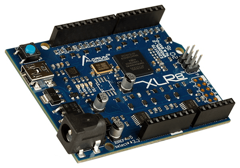
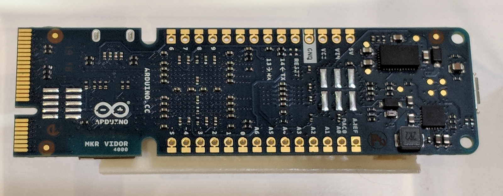
Hackaday brought you a first look the Arduino MKR Vidor 4000 when it announced. Arduino sent over one of the first boards so now we finally have our hands on one! It’s early and the documentation is still a bit sparse, but we did get it up and running to take the board through some hello world exercises. This article will go over what we’ve been able to figure out about the FPGA system so far to help get you up and running with the new hardware.

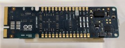
Just to refresh your memory, here’s what is on the Vidor board:

  • 8 MB SRAM
  • A 2 MB QSPI Flash chip — 1 MB allocated for user applications
  • A Micro HDMI connector
  • An MIPI camera connector
  • Wi-Fi and BLE powered by a U-BLOX NINA W10 Series device
  • MKR interface on which all pins are driven both by SAMD21 (32-bit ARM CPU) and FPGA
  • Mini PCI Express connector with up to 25 user programmable pins
  • The FPGA (an Intel/Altera Cyclone 10CL016) contains 16K Logic Elements, 504 KB of embedded RAM, and 56 18×18 bit HW multipliers

Sounds good. You can get more gory technical details over at Arduino and there’s even a schematic (.zip).

Documentation

Documentation is — so far — very hard to come by but the team is working to change that by the day. Here are the resources we’ve used so far (in addition to the schematic):

In addition, Arduino just released an example FPGA project for Quartus. I’ll explain what that means in a bit.

Get Up and Running with the Arduino Desktop IDE

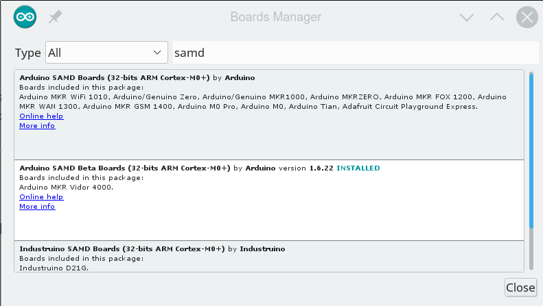
Despite the getting started guide, it doesn’t appear the libraries are usable from the cloud-based IDE, so we followed the instructions to load the beta board support for the MKR 4000 into our desktop IDE. Be aware that the instructions show the “normal” SAMD board package, but you actually want the beta which says it is for the MKR 4000. If you search for SAMD in the Boards Manager dialog, you’ll find it (see the second entry in the image below).


The libraries we grabbed as ZIP files from GitHub and used the install library from ZIP file option with no problems.

What’s the Code Look Like?

The most interesting part of this board is of course the inclusion of the FPGA which left us wondering what the code for the device would look like. Browsing the code, we were a bit dismayed at the lack of comments in all but the JTAG code. We decided to focus first on the VidorPeripherals repository and dug into the header file for some clues on how everything works.

Looking at VidorPeripherals.h, you can see that there’s a few interesting I/O devices include SPI, I2C, UART, reading a quadrature encoder, and NeoPixel. There’s also a few headers that don’t exist (and presumably won’t get the define to turn them on) so don’t get too excited by some of the header file names until you make sure they are really there.

Then we decided to try the example test code. The library provides a global FPGA object that you need to set up:

// Let's start by initializing the FPGA
if (!FPGA.begin()) {
    Serial.println("Initialization failed!");
    while (1) {}
}

// Let's discover which version we are running
int version = FPGA.version();
Serial.print("Vidor bitstream version: ");
Serial.println(version, HEX);

// Let's also ask which IPs are included in this bitstream
FPGA.printConfig();

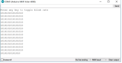
The output of this bit of code looks like this:

Vidor bitstream version: 1020107
number of devices 9
1 01000000 MB_DEV_SF
1 02000000 MB_DEV_GPIO
4 04000000 MB_DEV_I2C
6 05000000 MB_DEV_SPI
8 06000000 MB_DEV_UART
1 08000000 MB_DEV_SDRAM
4 09000000 MB_DEV_NP
11 0A000000 MB_DEV_ENC
0 0B000000 MB_DEV_REG

In many cases, the devices provided by the FPGA are pretty transparent. For example, here’s another snip from the example code:

// Ok, so we know now that the FPGA contains the extended GPIO IP
// The GPIO pins controlled by the FPGA start from 100
// Please refer to the online documentation for the actual pin assignment
// Let's configure pin A0 to be an output, controlled by the FPGA
FPGA.pinMode(33, OUTPUT);
FPGA.digitalWrite(33, HIGH);

// The same pin can be read by the SAMD processor :)
pinMode(A0, INPUT);
Serial.print("Pin A0 is ");
Serial.println(digitalRead(A0) == LOW ? "LOW" : "HIGH");

FPGA.digitalWrite(33, LOW);
Serial.print("Pin A0 is ");
Serial.println(digitalRead(A0) == LOW ? "LOW" : "HIGH");

That’s easy enough and it is nice that the pins are usable from the CPU and FPGA. We couldn’t find the documentation mapping the pins, but we assume it is coming.

Using, say, an extra serial interface is easy, too:

SerialFPGA1.begin(115200);
while (!SerialFPGA1);
SerialFPGA1.println("test");

Bitstream

So where’s the FPGA code? As far as you can tell, this is just a new Arduino with a lot of extra devices that connect through this mysterious FPGA object. The trick is that the FPGA code is in the library. To see how it works, let’s talk a little about how an FPGA operates.

When you write a program in C, that’s not really what the computer looks at, right? The compiler converts it into a bunch of numbers that tell the CPU to do things. An FPGA is both the same and different from that. You write your program — usually in a hardware design language like Verilog or VHDL. You compile it to numbers, but those numbers don’t get executed like a CPU does.

The best analogy I’ve been able to think of is that an FPGA is like one of those old Radio Shack 100-in-1 electronic kits. There are a bunch of parts on a board and some way to connect them with wires. Put the wires one way and you have a radio. Put them another way and you have a burglar alarm. Rewire it again and you have a metal detector. The numbers correspond to wires. They make connections and configure options in the FPGA’s circuitry. Unless you’ve built a CPU, there’s nothing in there examining and acting on the numbers like there would be with a CPU.

The numbers that come out of an FPGA tool is usually called a bitstream. Someone has to send that bitstream to an FPGA like the Cyclone onboard the Arduino every time it powers up. That someone is usually a memory device on the board, although the CPU can do it, too.

So that leads to two questions: Where is the bitstream? How does it get to the FPGA?

The answer to the first question is easy. If you look on Github, you’ll see in the library there is a file called VidorBase.cpp. It has the following lines:

__attribute__ ((used, section(".fpga_bitstream")))
const unsigned char bitstream[] = {
    #include "app.ttf"
};

What this means if there is an array called bitstream that the linker will put it in a specially marked section of memory. That array gets initialized with app.ttf which is just an ASCII file full of numbers. Despite the name, it is not a TrueType font. What do the numbers mean? Hard to say, although, in theory, you could reverse engineer it just like you can disassemble binary code for a CPU. However, it is the configuration required to make all the library calls we just talked about work.

The second question about how it gets to the FPGA configuration is a bit of a mystery. As far as we can tell, the bootloader understands that data in that section should get copied over to the FPGA configuration memory and does the copying for you. It isn’t clear if there’s a copy in the main flash and a copy in the configuration flash but it seems to work transparently in any event.

There’s a checksum defined in the code but we changed it and everything still worked. Presumably, at some point, the IDE or the bootloader will complain if you have the wrong checksum, but that doesn’t appear to be the case now.

By the way, according to the Arduino forum, there are actually two bitstreams. One that loads on power-up that you would rarely (if ever) change. Then there is another that is the one included with the library. You can double-click the reset button to enter bootloader mode and we suspect that leaves the FPGA initialized with the first bitstream, but we don’t know that for sure. In bootloader mode, though, the red LED onboard has a breathing effect so you can tell the double click works.

What about my FPGA Code?

This isn’t great news if you were hoping for an easy Arduino-like way to do your own FPGA development in Verilog or VHDL. Intel will give you a copy of Quartus Prime which will generate bitstreams all day for you. We think — but we aren’t sure — that the ASCII format is just a raw conversion from binary of the bitstream files.

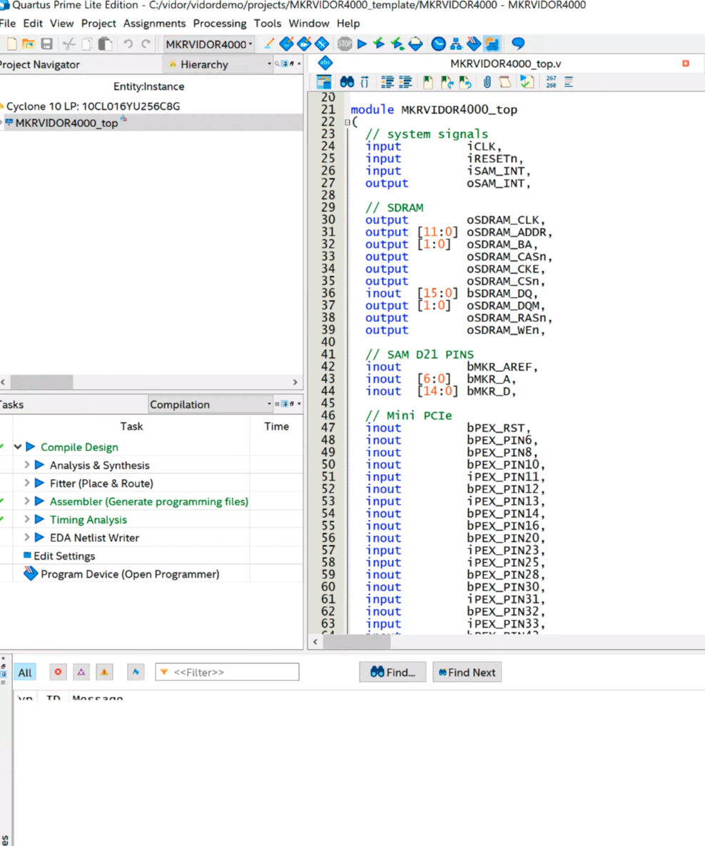
Very recently, Arduino provided a Quartus project that would create a bitstream. This provides a few key pieces of the puzzle, like the constraint file that lets the FPGA compiler find the different parts on the board.

However, even with that project, you still have some reverse engineering to do if you want to get started. Why? Here’s what Arduino says about loading your own FPGA code (we added the emphasis):

Quartus will produce a set of files under the output_files directory in the project folder. In order to incorporate the FPGA in the Arduino code you need to create a library and preprocess the ttf file generated by Quartus so that it contains the appropriate headers required by the software infrastructure. Details of this process will be disclosed as soon as the flow is stable.

Programming the FPGA is possible in various ways:

  • Flashing the image along with Arduino code creating a library which incorporates the ttf file
  • Programming the image in RAM through USB Blaster (this requires mounting the FPGA JTAG header). this can be done safely only when SAM D21 is in bootloader mode as in other conditions it may access JTAG and cause a contention
  • Programming the image in RAM through the emulated USB Blaster via SAM D21 (this component is pending release)

In addition, the repository itself says that some key pieces are missing until they can work out licensing or clean up the code. So this gets us closer, but you’d still need to reverse engineer the header from the examples and/or figure out how to force the processor off the JTAG bus. The good news is it sounds like this information is coming, it just isn’t here yet.

Of course, you are going to need to understand a lot more to do anything significant. We know the FPGA is set in the AS configuration mode. We also asked Arduino about the clock architecture of the board and they told us:

[The CPU] has its own clock which is used to generate a 48 MHz reference clock that is fed to the FPGA (and that can be removed at any time to “freeze” fpga). In addition to this reference clock, [the] FPGA has an internal RC oscillator which can’t be used as [a] precise timing reference for tolerance issues but can be used in case you don’t want [the CPU] to produce the reference clock.

Of course, the FPGA has a number of PLLs onboard that can take any valid clock and produce other frequencies. For example, in the vision application, Arduino demonstrated, the 48 MHz clock is converted into 24 MHz, 60 MHz, 100 MHz, and 120 MHz clocks by PLLs.

Mix and Match?

One thing that is disappointing is that — at least for now — you won’t be able to mix and match different FPGA libraries. There is exactly one bitstream and you can’t just jam them together.  Although FPGAs can often be partially configured, that’s a difficult technique. But we were a little surprised that the IDE didn’t understand how to take libraries with, for example, EDIF design files for IP that would all get compiled together. That way I could pick the Arduino UART and mix it with the Hackaday PWM output module along with my own Verilog or VHDL.

The way things are structured now you will have one bitstream that is precompiled by another tool (probably Quartus for the foreseeable future). It will match up with a particular C++ library. And that’s it. Doesn’t matter how much of the FPGA is left over or how much of it you really use, you will use it all for the one library.

Of course, you can load another library but it is going to replace the first one. So you only get one set of functions at a time and someone else gets to decide what’s in that set. If you roll your own, you are going to have to roll your own all the way.

What’s Next?

It is still early for the Arduino Vidor. We are hopeful we’ll get the tools and procedures necessary to drop our own FPGA configurations in. It would be great, too, if the stock libraries were available in source format including the Verilog HDL. The recent GitHub release shows quite a bit, although it isn’t all of the examples, it is probably enough if we get the rest of the information.

As for a more intuitive interface, we don’t know if that’s in the cards or not. We don’t see much evidence of it, although posts on the Arduino forum indicate they will eventually supply an “IP Assembler” that will let you compose different modules into one bitstream. We don’t know if that will only work with “official” modules or not. However, we know the Arduino community is very resourceful so if we don’t get a good ecosystem it will not surprise us if someone else makes it happen. Eventually.

For now, we will continue to play with the existing bitstreams that become available. There are some neat new features on the CPU, too. For example, you can map two of the unused serial modules.  There’s a hardware-based cooperative multitasking capability. As more details on the FPGA emerge, we’ll keep you posted and if you learn something, be sure to leave word in the comments so everyone can benefit.

Video of the Arduino FPGA Board Demo at Maker Faire

This week, Arduino announced a lot of new hardware including an exceptionally interesting FPGA development board aimed at anyone wanting to dip their toes into the seas of VHDL and developing with programmable logic. We think it’s the most interesting bit of hardware Arduino has released since their original dev board, and everyone is wondering what the hardware actually is, and what it can do.

This weekend at Maker Faire Bay Area, Arduino was out giving demos for all their wares, and yes, the Arduino MKR Vidor 4000 was on hand, being shown off in a working demo. We have a release date and a price. It’ll be out next month (June 2018) for about $60 USD.

But what about the hardware, and what can it do? From the original press releases, we couldn’t even tell how many LUTs this FPGA had. There were a lot of questions about the Mini PCIe connectors, and we didn’t know how this FPGA would be useful for high-performance computation like decoding video streams. Now we have the answers.

The FPGA on board the Arduino Vidor is an Altera Cyclone 10CL016. This chip has 16k logic elements, and 504 kB memory block. This is on the low end of Altera’s FPGA lineup, but it’s still no slouch. In the demo video below, it’s shown decoding video and identifying QR codes in real time. That’s pretty good for what is effectively a My First FPGA board.

Also on board the Vidor is a SAMD21 Cortex-M0+ microcontroller and a uBlox module housing an ESP-32 WiFi and Bluetooth module. This is a really great set of chips, and if you’re looking to get into FPGA development, this might just be the board for you. We haven’t yet seen the graphic editor that will be used to work with IP for the FPGA (for those who don’t care to write their own VHDL or Verilog), but we’re looking forward to the unveiling of that new software.

Arduino Just Introduced an FPGA Board, Announces Debugging and Better Software

Today ahead of the Bay Area Maker Faire, Arduino has announced a bevy of new boards that bring modern features and modern chips to the Arduino ecosystem.

Most ambitious of these new offerings is a board that combines a fast ARM microcontroller, WiFi, Bluetooth, and an FPGA. All this is wrapped in a package that provides Mini HDMI out and pins for a PCIe-Express slot. They’re calling it the Arduino MKR Vidor 4000.

Bringing an FPGA to the Arduino ecosystem is on the list of the most interesting advances in DIY electronics in recent memory, and there’s a lot to unpack here. FPGA development boards aren’t new. You can find crates of them hidden in the storage closet of any University’s electronics lab. If you want to buy an FPGA dev board, the Terasic DE10 is a good starter bundle, the iCEstick has an Open Source toolchain, and this one has pink soldermask. With the release of the MKR Vidor, the goal for Arduino isn’t just to release a board with an FPGA; the goal is to release a tool that allows anyone to use an FPGA.

The key to democratizing FPGA development is Arduino’s work with the Arduino Create ecosystem. Arduino Create is the company’s online IDE that gives everyone the ability to share projects and upload code with Over-the-Air updates. The MKR Vidor will launch with integration to the Arduino Create ecosystem that includes a visual editor to work with the pre-compiled IP for the FPGA. That’s not to say you can’t just plug your own VHDL into this board and get it working; that’s still possible. But Arduino would like to create a system where anyone can move blocks of IP around with a tool that’s easy for beginners.

A Facelift for the Uno WiFi

First up is the brand new Arduino Uno WiFi. While there have been other boards bearing the name ‘Arduino Uno WiFi’ over the years, a lot has changed in the world of tiny radio modules and 8-bit microcontrollers over the past few years. The new Arduino Uno WiFi is powered by a new 8-bit AVR, the ATMega4809. The ATMega4809 is a new part announced just a few months ago, and is just about what you would expect from the next-generation 8-bit Arduino; it runs at 20MHz, has 48 kB of Flash, 6 kB of SRAM, and it comes in a 48-pin package. The ATMega4809 is taking a few lattices of silicon out of Microchip’s playbook and adds Custom Configurable Logic. The CCL in the new ATMega is a peripheral that is kinda, sorta like a CPLD on chip. If you’ve ever had something that could be more easily done with logic gates than software, the CCL is the tool for the job.

But a new 8-bit microcontroller doesn’t make a WiFi-enabled Arduino. The wireless power behind the new Arduino comes from a custom ESP-32 based module from u-blox. There’s also a tiny crypto chip (Microchip’s ATECC508A) so the Uno WiFi will work with AWS. The Arduino Uno WiFi will be available this June.

But this isn’t the only announcement from the Arduino org today. They’ve been hard at work on some killer features for a while now, and now they’re finally ready for release. What’s the big news? Debuggers. Real debuggers for the Arduino that are easy to use. There are also new boards aimed at Arduino’s IoT strategy.

The Future of Arduino

As you would expect in the world of embedded development, the future is IoT. Last week, Arduino announced the release of two new boards, the MKR WiFi 1010 and the MKR NB 1500. The MKR WiFi 1010 features a SAMD21 Cortex-M0+ microcontroller and a u-blox module (again featuring an ESP-32) giving the board WiFi. The MKR NB 1500 is designed for cellular networks and features the same SAMD21 Cortex-M0+ microcontroller found in the MKR WiFi 1010, but also adds a u-blox cellular module that will connect to LTE networks using Narrowband IoT, but the module does also support Cat M1 networks.

But IoT isn’t the only thing Arduino has been working on. On the leadup to the World Maker Faire this weekend, I had the opportunity to speak with Fabio Violante, CEO of Arduino, and Massimo Banzi, Co-founder of Arduino, and what I heard was remarkable. There’s going to be an update to the Arduino IDE soon, and real debugging is coming to the Arduino ecosystem. This is a significant development in Arduino’s software efforts, and when Fabio was appointed CEO last July, this was the first thing he wanted to do.

Also on deck for upcoming bits of hardware is a slow upgrade from ARM Cortex-M0 parts to Cortex-M4 parts. While this change isn’t exactly overdue, it is a direct result of the ever-increasing power of available microcontrollers. The reason for this change is the growing need for more compute power on embedded platforms, and simply the fact that more powerful chips are cheaper now.

Massimo, Fabio, and the rest of the Arduino team will be showing off their latest wares at Maker Faire Bay Area this weekend, and we will be posting updates. The FPGA Arduino — the MKR Vidor 4000 — will be on display running a computer vision demo, and there will, of course, be fancy new boards on hand. We’ll be posting updates so keep your eye on Hackaday!

Hack a Day 18 May 16:03