Tutorial – Arduino and the TI ADS1110 16-bit ADC
Learn how to use the TI ADS1110 16-bit ADC with Arduino in chapter fifty-three of my Arduino Tutorials. The first chapter is here, the complete series is detailed here.
Updated 02/07/2013
Introduction
Moving on from the last chapter where we explained an 8-bit ADC, in this instalment we have the Texas Instruments ADS1110 – an incredibly tiny but useful 16-bit analogue-to-digital converter IC. It can operate between 2.7 and 5.5 V so it’s also fine for Arduino Due and other lower-voltage development boards. This is a quick guide to get you going with the ADS1110 ready for further applications. Before continuing any further, please download the data sheet (pdf) as it will be useful and referred to during this tutorial. The ADS1110 gives you the option of a more accurate ADC than offered by the Arduino’s 10-bit ADCs – and it’s relatively easy to use. The only block for some is the package type – it’s only available in SOT23-6:

So unless you’re making a customised PCB, some sort of breakout will be required. One useful example is the Schmartboard we reviewed earlier:

The ADS1110 uses the I2C bus for communication, so if this is new to you – please review the I2C tutorials before continuing. And as there’s only six pins you can’t set the bus address – instead, you can select from six variants of the ADS1110 – each with their own address (see page two of the data sheet). As you can see the in the photo above, ours is marked “EDO” which matches to the bus address 1001000 or 0x48h. And with the example circuits we’ve used 10kΩ pull-up resistors on the I2C bus. You can use the ADS1110 as either a single-ended or differential ADC – But first we need to examine the configuration register which is used to control various attributes, and the data register.
Configuration register
Turn to page eleven of the data sheet. The configuration register is one byte in size, and as the ADS1110 resets on a power-cycle – you need to reset the register if your needs are different to the defaults. The data sheet spells it out quite neatly… bits 0 and 1 determine the gain setting for the PGA (programmable gain amplifier). If you’re just measuring voltages or experimenting, leave these as zero for a gain of 1V/V. Next, the data rate for the ADS1110 is controlled with bits 2 and 3. If you have continuous sampling turned on, this determines the number of samples per second taken by the ADC.
After some experimenting with an Arduino Uno we found the values returned from the ADC were a bit off when using the fastest rate, so leave it as 15 SPS unless required otherwise. Bit 4 sets either continuous sampling (0) or one-off sampling (1). Ignore bits 5 and 6, however they’re always set as 0. Finally bit 7 – if you’re in one-off sampling mode, setting it to 1 requests a sample – and reading it will tell you if the returned data is new (0) or old (1). You can check that the value measured is a new value – if the first bit of the configuration byte that comes after the data is 0, it’s new. If it returns 1 the ADC conversion hasn’t finished.
Data register
As the ADS1110 is a 16-bit ADC, it returns the data over two bytes – and then follows with the value of the configuration register. So if you request three bytes the whole lot comes back. The data is in “two’s complement” form, which is a method of using signed numbers with binary. Converting those two bytes is done by some simple maths. When sampling at 15 SPS, the value returned by the ADS1110 (not the voltage) falls between -32768 and 32767. The higher byte of the value is multiplied by 256, then added to the lower byte – which is then multiplied by 2.048 and finally divided by 32768. Don’t panic, as we do this in the example sketch below.
Single-ended ADC mode
In this mode you can read a voltage that falls between zero and 2.048 V (which also happens to be the inbuilt reference voltage for the ADS1110). The example circuit is simple (from the data sheet):
 Don’t forget the 10kΩ pull-up resistors on the I2C bus. The following sketch uses the ADS1110 in the default mode, and simply returns the voltage measured:
// Example 53.1 - ADS1110 single-sided voltmeter (0~2.048VDC)
#include "Wire.h"
#define ads1110 0x48
float voltage, data;
byte highbyte, lowbyte, configRegister;
void setup()
{
Serial.begin(9600);
Wire.begin();
}
void loop()
{
Wire.requestFrom(ads1110, 3);
while(Wire.available()) // ensure all the data comes in
{
highbyte = Wire.read(); // high byte * B11111111
lowbyte = Wire.read(); // low byte
configRegister = Wire.read();
}
data = highbyte * 256;
data = data + lowbyte;
Serial.print("Data >> ");
Serial.println(data, DEC);
Serial.print("Voltage >> ");
voltage = data * 2.048 ;
voltage = voltage / 32768.0;
Serial.print(voltage, DEC);
Serial.println(" V");
delay(1000);
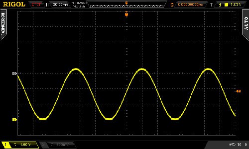
}Once uploaded, connect the signal to measure and open the serial monitor – you’ll be presented with something similar to:

If you need to alter the gain of the internal programmable gain amplifier of the ADC – you’ll need to write a new byte into the configuration register using:
Wire.beginTransmission(ads1110);
Wire.write(configuration byte);
Wire.endTransmission();
before requesting the ADC data. This would be 0x8D, 0x8E or 0x8F for gain values of 2, 4 and 8 respectively – and use 0x8C to reset the ADS1110 back to default.
Differential ADC mode
In this mode you can read the difference between two voltages that each fall between zero and 5 V. The example circuit is simple (from the data sheet):

We must note here (and in the data sheet) that the ADS1110 can’t accept negative voltages on either of the inputs. You can use the previous sketch for the same results – and the resulting voltage will be the value of Vin- subtracted from Vin+. For example, if you had 2 V on Vin+ and 1 V on Vin- the resulting voltage would be 1 V (with the gain set to 1).
Conclusion
Once again I hope you found this of interest, and possibly useful. And if you enjoy my tutorials, or want to introduce someone else to the interesting world of Arduino – check out my new book “Arduino Workshop” from No Starch Press.

In the meanwhile have fun and keep checking into tronixstuff.com. Why not follow things on twitter, Google+, subscribe for email updates or RSS using the links on the right-hand column? And join our friendly Google Group – dedicated to the projects and related items on this website. Sign up – it’s free, helpful to each other – and we can all learn something.
The post Tutorial – Arduino and the TI ADS1110 16-bit ADC appeared first on tronixstuff.