2-Layered PCB with a Laser? Nah, Toner Transfer
I tried using the laser to remove some spray paint, and... I declare it a dud. Two major factors stymied this process for me for the moment:
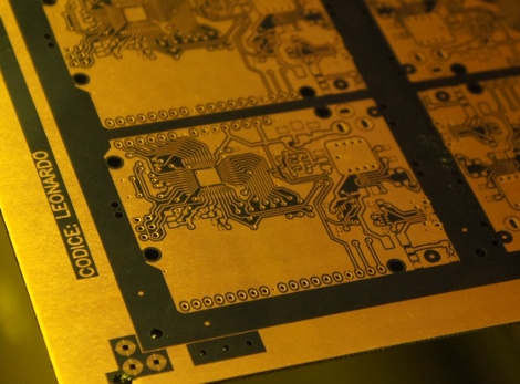
 Impatient as usual, I used my regular method: laser printer toner transfer. Determined to make a 2-sided board work, I spent a while aligning corner crop marks and pre-taping the paper with the toner before laminating it to the copper. The toner transfer was spectacular-- just perfect laminating it ten times (5 up, 5 down), but the top-bottom alignment, while close, may not be close enough. At this point it's etched and drilled, but there are still bridges and the misalignment will make assembly an adventure.
Looking at guides online, (especially the tutorial at An Engineer's Life which so many people are linking to today,) it does seem like most people use a photographic process and abandon toner transfer when they go for double-sided and SMD. Before going that route, I want to take toner transfer further though-- I've had such good results so far, the only issue is top-bottom alignment. The biggest sources of alignment error:
- I didn't have the right spray paint (matte black) nor the right environment (dry and warm) for the paint I did have. What I did get to stick to the copper had a very uneven surface.
- The laser is... finicky. I can't tell if the layers were wildly inconsistent, if the paint behaved differently as it dried, or if maybe the laser had trouble, not liking the cold temperature or moist environment. I never can tell if it's about to give up.
Looking at guides online, (especially the tutorial at An Engineer's Life which so many people are linking to today,) it does seem like most people use a photographic process and abandon toner transfer when they go for double-sided and SMD. Before going that route, I want to take toner transfer further though-- I've had such good results so far, the only issue is top-bottom alignment. The biggest sources of alignment error:
- Top-bottom alignment of printed out patterns. A light table, some magnets, and tape should do the trick-- I need to see the registration targets better.
- The laminator binds and jerks sometimes, which could distort the pattern slightly. It's hard to tell without sending through a test image, but it seems like time to take apart the laminator and see about modding it to separate the rollers a hair.