

555-Based Dimmer 3D Circuit
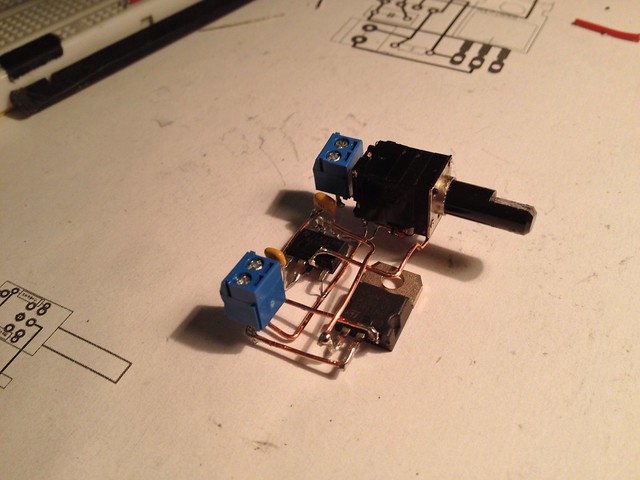
It's a dimmer circuit: a 555-timer-based PWM generator driving a high power MOSFET. I kept it simple and focused on a method, not on making anything particularly fancy.
I edited a schematic for a board I'd built earlier, adding a scrounged 10k audio potentiometer with switch. The parts list was short:
- 10k potentiometer with switch,
- 2 2-pin screw terminals (input and output),
- NE555 8-pin chip,
- fat npn MOSFET like a TIP120,
- 2 1N4148 diodes,
- 2 capacitors: .1uF and 1uF,
- 330 ohm resistor
- Put the major components where you want them first,
- Pack the rest of the components in paying attention to keeping traces short.
- Small 2-lead components can fit later, with one lead overlapping its signal, the other reached by a branch made from its lead.
- Lay out a few long traces that hit the most pins and cover the most ground first. Try to get those traces in a straight line or aligned in an L- or S- or U- arrangement, more or less.
- Avoid branching, unless the branch can be a component's lead.
- Small kinks and zig-zags are OK and may be built with straighter wire segments later, with pins bent to get where they need to be.
- Don't think much about top/bottom layering and about crossing lines. There will be room to cross a wire here or there. Try not to cross, but you can worry about top and bottom later.
- Print out a sheet to see the circuit different ways, running the same sheet through the printer, taking advantage of the print options:
- Aligned top center, scale 2 or 3 (what will fit), with all layers drawn.
- Aligned lower left, scale 1, with all layers,
- Aligned lower right, scale 1, just the traces.
- Note: also print scale 1 mirrored versions too, of all layers and traces only, to see things from the bottom, which is how things are soldered.
- In the trace-only print-out, number the longest traces to make wires for them.
- Strip a length of stripped solid-core wire for each long trace. Bend them to shape with pliers, clipping to length, using the trace-only print as the pattern.
- Small kinks in the pattern don't generally need to be bent-- wires and pins will bend during soldering.
- Clip leads after soldering, unless it has to butt up as a T. It's easy to clip after soldering, and wires can shift during soldering.

[original story: Jeff's Arduino Blog]